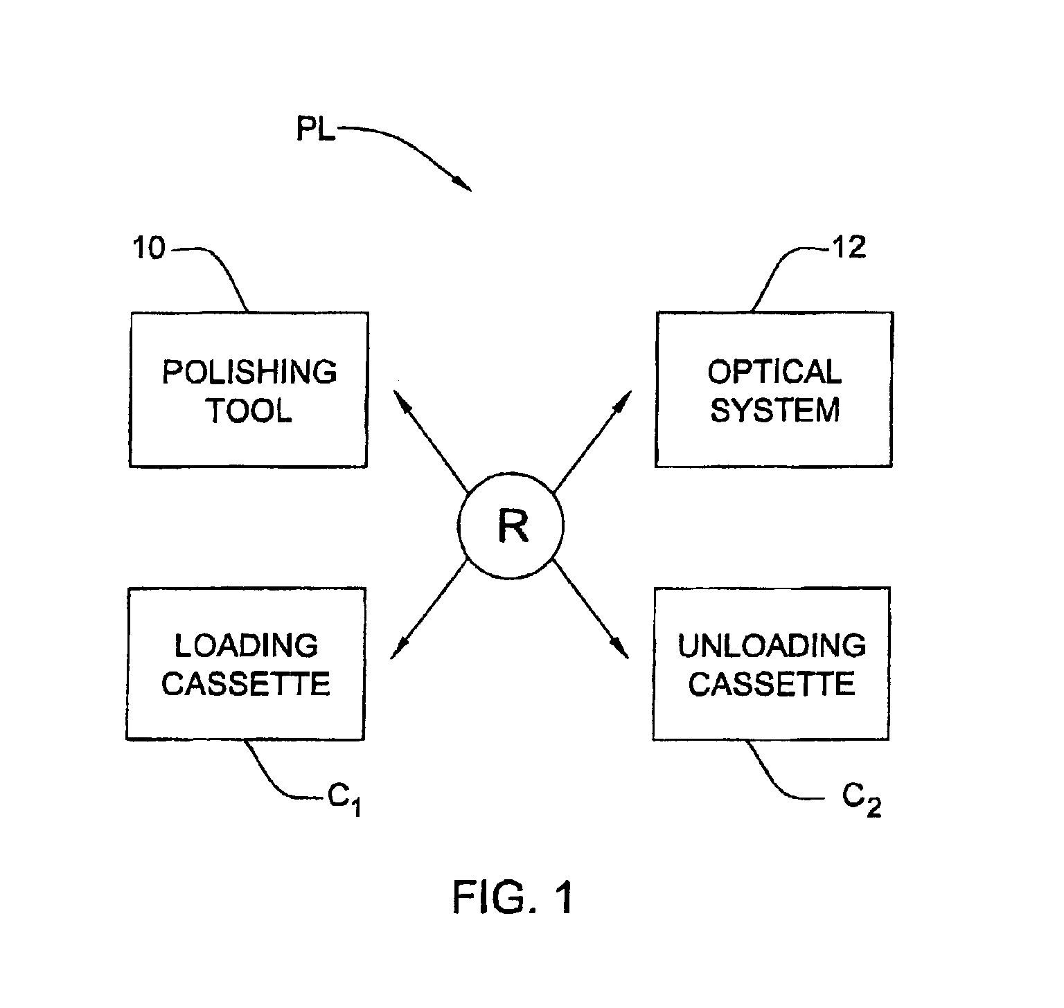
Method and system for monitoring a process of material removal from the surface of a patterned structure
a technology of patterned structure and surface removal, applied in the field of optical monitoring techniques, can solve the problems of unsatisfactory effects of residue, erosion and corrosion, add to polishing difficulties, scratching and embedding particles,
- Summary
- Abstract
- Description
- Claims
- Application Information
AI Technical Summary
Benefits of technology
Problems solved by technology
Method used
Image

Examples
example 1
Absolute Dishing Measurement as a Combination of Phase Mapping (Imaging) and Spectrophotometric Measurement
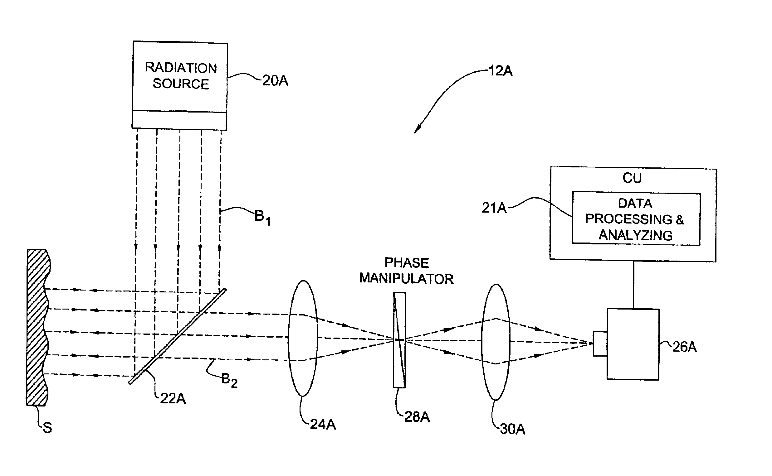
[0073]To implement this measurement the optical system of FIG. 3B is applied to the structure of FIG. 2A or FIG. 2C.
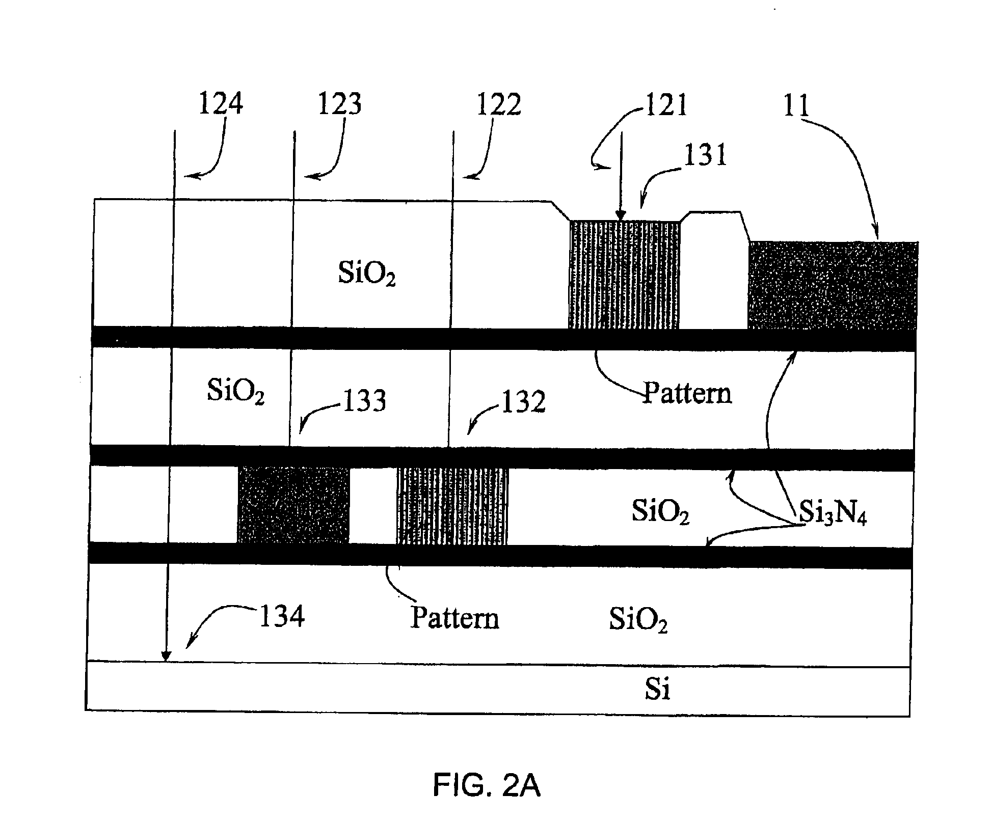
[0074]Step 1: Spectrophotometric measurement allows extraction of data about the reference stack parameters (i.e., reflective properties of the layer stacks in the measured sites). Using these stack parameters, the phase φUP of the reflected wave at the upper interface of the reference stack can be calculated. Reference pad can be either in the upper layer (pad 131 in FIG. 2A or pad 331 in FIG. 2C), or in the underneath layers of the structure (pads 132 and 133 in FIG. 2A). Spectrophotometric measurement is applied to the selected site (site of interest), which is a pad in the dishing measurement application, i.e., the pad 11 in FIG. 2A or pad 332 in FIG. 2C in the present examples, and applied to at least one of the following points (reference sites): point 331 a...
example 2
Absolute Erosion Measurement as a Combination of Phase Mapping (Imaging) and Spectrophotometric Measurement
[0083]In the present example, the optical monitoring system of FIG. 3B is applied to the structure of FIG. 2B and FIG. 2C.
[0084]Step 1: As indicated above, the spectrophotometric measurement allows extraction of data about the reference stack parameters, and using these stack parameters the phase φUP of the reflected wave at the upper interface of the reference stack can be calculated. Reference pad can be either in the upper layer (site 231 in FIG. 2B or site 332 in FIG. 2C) or in the underneath layers (sites 232 and 233 in FIG. 2B). The spectrophotometric measurement is done in the site of interest (for metal CMP this is a pad in the form of spaced-apart metal-containing regions in the erosion measurement applications, which it pad 21 in the example of FIG. 2B; for dielectric CMP this is a pad in the form of spaced-apart different dielectric regions, which are silicon dioxide...
example 3
Absolute Dishing Measurement Using Phase Mapping (Imaging) Only
[0090]For these measurements, the optical system of FIG. 3A is used.
[0091]Step 1: This measurement, scheme includes measurement of the phase difference Δφ on the pad of interest and the reference pad (Cu or W), wherein the reference pad is small enough (from 2×2 um2 to 10×10 um2), i.e., has negligible dishing effect as compared to the pad of interest. In this case, the phase shift of the reflected light is the same on the reference pad and the pad of interest due to the substantially fill reflection, of incident light by the reference pad and pad of interest in the upper layer.
[0092]Step 2: Dishing is calculated according to the following expression: Dishing=λΔφ4π n.
[0093]The reference pad can be of an arbitrary shape (square, line, etc.). To improve the accuracy the metal recess effect can also be taken into account.
PUM
 Abstract
Description
Claims
Application Information
 - R&D
- Intellectual Property
- Life Sciences
- Materials
- Tech Scout
- Unparalleled Data Quality
- Higher Quality Content
- 60% Fewer Hallucinations
Browse by: Latest US Patents, China's latest patents, Technical Efficacy Thesaurus, Application Domain, Technology Topic, Popular Technical Reports.
© 2025 PatSnap. All rights reserved.Legal|Privacy policy|Modern Slavery Act Transparency Statement|Sitemap|About US| Contact US: help@patsnap.com