
Eliminating substrate noise by an electrically isolated high-voltage I/O transistor

a high-voltage i/o transistor and substrate noise technology, applied in the direction of semiconductor devices, electrical apparatus, basic electric elements, etc., can solve the problems of increasing the effect of noise coupling, affecting the performance of analog circuits, and economic unattractive, and achieves the effect of higher resistivity

Inactive Publication Date: 2005-04-05
TEXAS INSTR INC
View PDF15 Cites 20 Cited by
  • Summary
  • Abstract
  • Description
  • Claims
  • Application Information

AI Technical Summary

Benefits of technology

It is a technical advantage of the present invention that there are several options for designing the buried layer and the electrical contact to the resulting isolated base of the MOS transistor:
that there are several options for designing the buried layer and the electrical contact to the resulting isolated base of the MOS transistor:
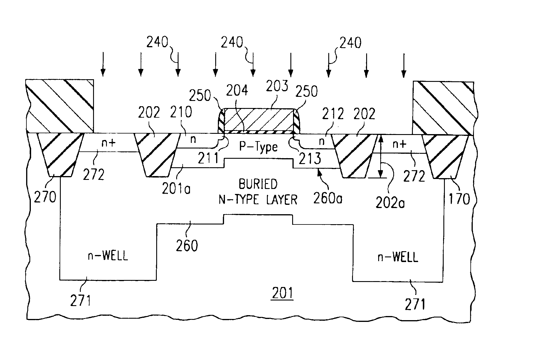
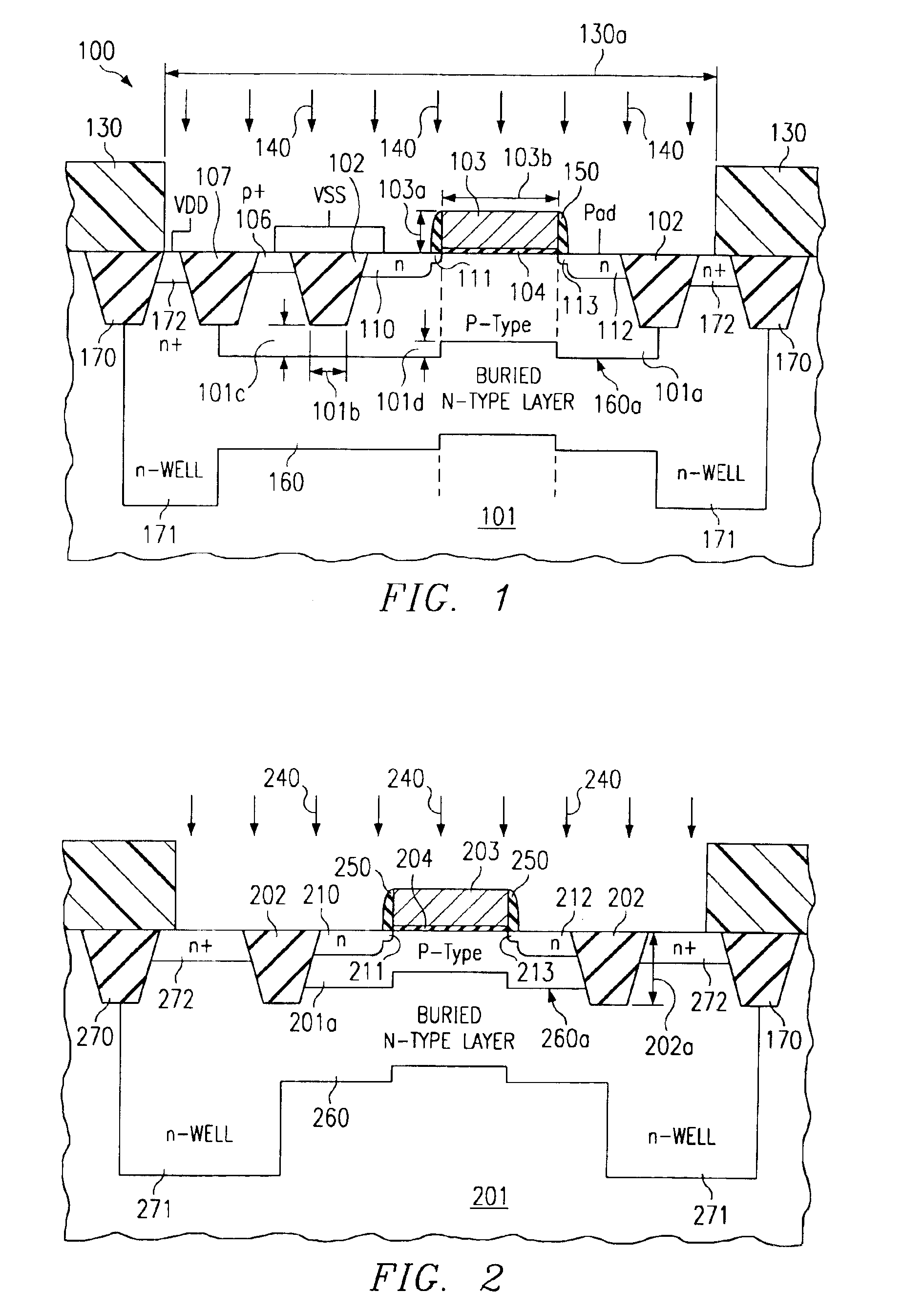
In the first embodiment of the invention, the buried layer extends vertically deeper from the surface than the electrical isolation region, thereby enabling a separate contact to the electrically isolated near-surface portion of the semiconductor region.
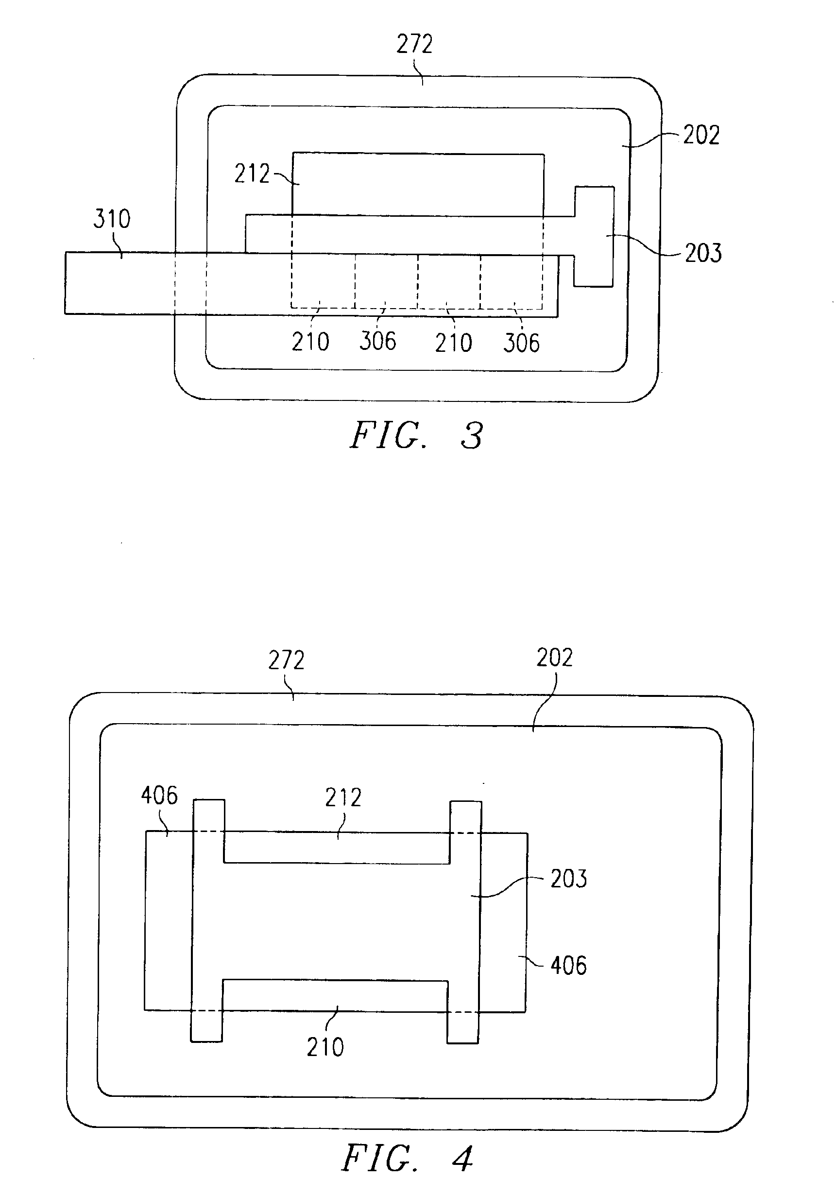
In the second embodiment of the invention, the buried layer extends vertically from the surface not as deep as the electrical isolation region, thereby enabling contacts to the electrically isolated near-surface portion of the semiconductor region in the shape of a body-tied source. This body-tied source is configured to provide a dual-function contact region to the MOS transistor source, and to the electrically isolated near-surface portion of the semiconductor region.
In the third embodiment of the invention, the buried layer extends vertically from the surface not as deep as the electrical isolation region, thereby enabling contacts to the electrically isolated near-surface portion of the semiconductor region in the shape of an angular-structured gate of the MOS transistor. This angular-structured gate is configured to include an H-shape or a T-shape such that its directly adjacent regions provide contacts to the source, drain, and near-surface portion of the semiconductor region.
It is an essential aspect of the invention to use the photomask step, which is needed for implanting the low energy ions in order to create the extended source and drain, for the additional process step of implanting at high energy and high dose the ions needed to create the buried layer. This economical feature renders the additional high-energy ion implant step and thus the formation of an electrically isolated high-voltage I / O transistor exceedingly inexpensive.

Problems solved by technology

Consequently, since analog circuits share the same substrate with high-speed digital circuits, electrical noise created by the high-speed operation is coupled between the circuits and may affect the performance of the analog circuits.
As the frequency of the operational digital circuit increases, and transistor dimensions are reduced, the effect of the noise coupling is becoming more and more serious.
Unfortunately, the proposed substrate noise remedies include designs requiring additional silicon real estate area, or additional photomask steps.
The costs connected with these additional design and fabrication steps make them economically unattractive.

Method used


Image

  • Eliminating substrate noise by an electrically isolated high-voltage I/O transistor
  • Eliminating substrate noise by an electrically isolated high-voltage I/O transistor
  • Eliminating substrate noise by an electrically isolated high-voltage I/O transistor

Examples


first embodiment

Vertically, the position of the buried layer 160 relative to the surface depends on the energy of the implanted ions. In the invention, which is depicted in FIG. 1, the buried layer edge 160a nearest the surface is deeper, i.e. farther away, from the surface than the bottom of the electrical isolation regions 102. This fact results in an electrically isolated p-type region 101a continuous under one portion of isolation region 102; this connecting portion is marked 101b in FIG. 1. The thickness 101c of the connecting portion is a function of the energy of the implanted n-type ions.

This continuity feature, in turn, enables a separate p+-contact 106 to the electrically isolated near-surface portion 101a of the p-type semiconductor region. The geometrical extent of the contact region 106 is limited by an additional isolation region 107, which simultaneously serves as one of the limiting “markers” for n-well 171.

It may be mentioned that the thickness of the photoresist layer 130 is large...

second embodiment

In the invention, the electrical contact to the isolated region 201a is provided by the design of source 210 as a “body-tied source”. The structure of this body-tied-to-source is schematically illustrated in the top view of the transistor in FIG. 3. Equal numbers refer to equal entities in FIGS. 2 and 3. The n+ contact 272 to the n-well (and thus the buried n-type layer) completely surrounds the nMOS transistor; n+ contact 272 is electrically connected to Vdd. Nested within the n+ contact is the shallow trench isolation 202. Gate 203 of the nMOS transistor may be designed in a variety of different shapes convenient for layout and electrical connections. N+-type drain contact region 212 is electrically connected to the I / O pad as the high voltage contact. The (n+-type) source contact regions 210 alternate laterally with the (p+-type) body contact regions 306 (not shown in FIG. 2). Overlaid metal contact layer 310 joins the electrical contacts to source and body and provides the elect...

third embodiment

In the invention, the electrical contact to the isolated region 201a (the body) is provided by a design practiced in the silicon-on-insulator technology: The gate is structured in an “H”-shape or a “T”-shape. An example is illustrated in the schematic top view of FIG. 4 for an H-shaped gate of an nMOS transistor. Equal numbers refer to equal entities in FIGS. 2 and 4. The n+ contact 272 to the n-well (and thus the buried n-type layer) completely surrounds the nMOS transistor; n+ contact 272 is electrically connected to Vdd. Nested within the n+ contact is the shallow trench isolation 202. Gate 203 of the nMOS transistor may be designed in a variety of different shapes such as H-shape (as Shown in FIG. 4) or T-shape. N+-type drain contact region 212 is electrically connected to the I / O pad as the high voltage contact. N+-type source contact region 210 is connected to Vss. P+-type body contacts 406 are also connected to Vss.

By way of example for an nMOS transistor as shown in FIG. 2, ...


PUM


Abstract

On the surface of a semiconductor material of a first conductivity type 101a, a lateral MOS transistor 100 is described surrounded by a well 171 of the opposite conductivity type and, nested within the well, an electrical isolation region 102. The semiconductor region 101a embedding this transistor has a resistivity higher than the remainder of the semiconductor material 101 and further contains a buried layer 160 of the opposite conductivity type. This layer 160 extends laterally to the wells 171, thereby electrically isolating the near-surface portion of the semiconductor region from the remainder of the semiconductor material, and enabling the MOS transistor to operate as an electrically isolated high-voltage I / O transistor for circuit noise reduction, while having low drain junction capacitance.In the first embodiment of the invention (FIG. 1), the buried layer 171 extends vertically deeper from the surface than the electrical isolation region 102, thereby enabling a separate contact 106 to the electrically isolated near-surface portion 101a of the semiconductor region.

Description

FIELD OF THE INVENTIONThe present invention is related in general to the field of electronic systems and semiconductor devices, and more specifically to structures and fabrication methods for an electrically isolated high-voltage transistor operable to eliminate substrate noise.DESCRIPTION OF THE RELATED ARTIn mixed-signal integrated circuits (ICs), analog circuits are designed on the same semiconductor chip together with digital circuits. Consequently, since analog circuits share the same substrate with high-speed digital circuits, electrical noise created by the high-speed operation is coupled between the circuits and may affect the performance of the analog circuits. As the frequency of the operational digital circuit increases, and transistor dimensions are reduced, the effect of the noise coupling is becoming more and more serious.A recent study of the substrate noise and several types of guard rings designed for noise rejection, has been published by Hwan-Mei Cheng et al. (“A ...

Claims


Application Information

Patent Timeline
IPC IPC(8): H01L21/70H01L21/761H01L21/822H01L29/10H01L27/04H01L29/78
CPCH01L21/761H01L29/1083H01L29/7833
Inventor SALLING, CRAIG T.WU, ZHIQIANG
Owner TEXAS INSTR INC
Learn More