
Vertical color filter detector group and array

a detector group and array technology, applied in the field of active pixel image sensors, can solve the problems of inability to detect the image accurately, reduce the detection efficiency, so as to reduce the cost, reduce the cost, and reduce the effect of circuitry and wiring

Inactive Publication Date: 2005-03-08
FOVEON
View PDF22 Cites 56 Cited by
  • Summary
  • Abstract
  • Description
  • Claims
  • Application Information

AI Technical Summary

Benefits of technology

Color detector groups of the present invention can be configured into an array of color detector groups, such as a mosaic sensor group having two rows of color detector groups, each row having two color detector groups. In this embodiment, each color detector group is configured to read out only one wavelength band, but the color filters for blue, green and red are all active. The color filter responses of the detector layers in combination with the choice of which detector layer is connected to the read out circuit determines which wavelength band is sensed by a given detector group. The array of this embodiment produces a fixed color filter array pattern based on three colors. By reading out only one color per pixel location, significant reductions in circuitry and wiring can be realized resulting in higher yield and therefore reduced cost, and simplifying the interface to systems that require color sub-sampled data as input. Reduced circuitry and wiring per color detector group location also results in increased fill factor per pixel location, thus providing superior image sensor performance by increasing the signal to noise ratio and improving dynamic range.
In another embodiment, the present invention provides a mosaic detector group that allows a color filter array pattern, such as a Bayer pattern, to be switched between two different states. Switching the color filter array pattern enables increased resolution in interpolated images by capturing two color sub-sampled images and combining them. In addition, the ability to change the color filter array pattern simplifies integration of the array with other components of a system configured to work with a particular orientation or type of color filter array pattern. In this embodiment, color filter detector groups are configured in a mosaic detector group having two rows and two columns of color detector groups, each color detector group configured to read out two wavelength bands, but with the color filters for blue, green and red all active and further, the circuits for reading out the two wavelength bands sharing a common column output line. The column output lines are shared among color detector groups that lie along the same column of the mosaic detector group. Programming the mosaic detector group to switch between wavelength bands on each color detector group provides the switching between different color filter array states.
In yet another embodiment, color detector groups of the present invention can be configured in a mosaic detector group that uses color sub-sampling in two channels, but full sampling in a third channel. In this embodiment, the color detector group of the present invention is configured into a two row, two column array of detector groups, wherein each color detector group is configured to read out two wavelength bands, but with the color filters for blue, green, and red all active. The signals corresponding to each of the two wavelength bands are output on separate column output lines, the column output lines being shared by color detector groups that lie along the same column of the mosaic detector group. In this embodiment, two colors can be collected at each pixel location. In one case of this embodiment, the red and blue wavelength bands can be sub-sampled by sensing red or blue illumination at alternate color detector group locations within the detector group array, while the green wavelength band can be sensed at every location. This provides high resolution and reduced aliasing while still maintaining some of the benefits of reading out only two colors per pixel, the primary benefit being reduced complexity of readout circuits which leads to better yield and increased fill factor.
Each of the disclosed embodiments of arrays of color detector groups can optionally be modified by the addition of a pattern of optical color filters applied over the array. Using only a single filter material, an array with three detectors per detector group can be augmented to detect light with 4, 5, or 6 different spectral sensitivity ranges, to yield potentially improved color accuracy. The filter material may be an organic dye filter as in prior-art color image sensors, or it may be a layer than can be integrated into the semiconductor fabrication process, such as either a layer of polysilicon to absorb short wavelengths, or a stack of alternating oxide and nitride layers to shape the spectral response by interference effects. Other interference-based dielectric filter stacks are also possible in conjunction with the color detector groups of the present invention. While use of a single filter material permits up to 6 different spectral sensitivities, the present invention is in no way limited to the use of a single filter material, and color sensor arrays that employ color detector groups of the present invention in combination with color filters that have multiple different spectral transmission characteristics are possible and may be desirable for certain applications.

Problems solved by technology

Such sensors have the disadvantage of occupying a relatively large area per pixel as these sensors are tiled together in a plane.
In addition, reconstruction of a color image from such a sensor is computationally intensive and often results in images with artifacts, defects, or inferior resolution.
The device disclosed in the Carr patent has several shortcomings, the most notable being its large area, rendering it unsuitable for the image sensor density requirements of modern imaging systems.
The technology employed for contact formation to the buried infrared sensing diode is not suitable for modern imaging technology or extension to a 3-color sensor.
This requirement disadvantageously increases sensor area and complicates support circuits in the array.
The added circuit complexity makes it difficult to make an image sensor array that has the flexible color readout capabilities disclosed in this invention and makes it impossible to achieve the small pixel sizes required by many modern electronic imaging applications.
Among the shortcomings of this disclosure are difficult and non-standard manufacturing techniques, use of structures that prohibit high density of pixels, no ability to select different colors for read out, and inability to perform detection of three or more colors using a monolithic semiconductor substrate.
The performance of this sensor is limited by the poor color response of the double junction photodiode and by the fact that the n-well forms the cathode of both photodiodes, making this pixel design very susceptible to non-linear crosstalk between the color channels.
Additionally, the authors cite non-uniformity and process / fabrication constraints that limit the performance and potential benefits of this design.
None of the prior art discussed above provides any mechanism for dynamic control of the color filter array pattern.
Also, the aforementioned prior art does not enable choosing between full-measured color and sub-sampled color.
Further limitations are that the prior art discussed above does not disclose a practical way to make a color imaging array containing more than three distinct spectral sensitivities.

Method used


Image

  • Vertical color filter detector group and array
  • Vertical color filter detector group and array
  • Vertical color filter detector group and array

Examples


Embodiment Construction

Persons of ordinary skill in the art will realize that the following description of the present invention is illustrative only and not in any way limiting. Other embodiments of the invention will readily suggest themselves to such skilled persons having the benefit of this disclosure.

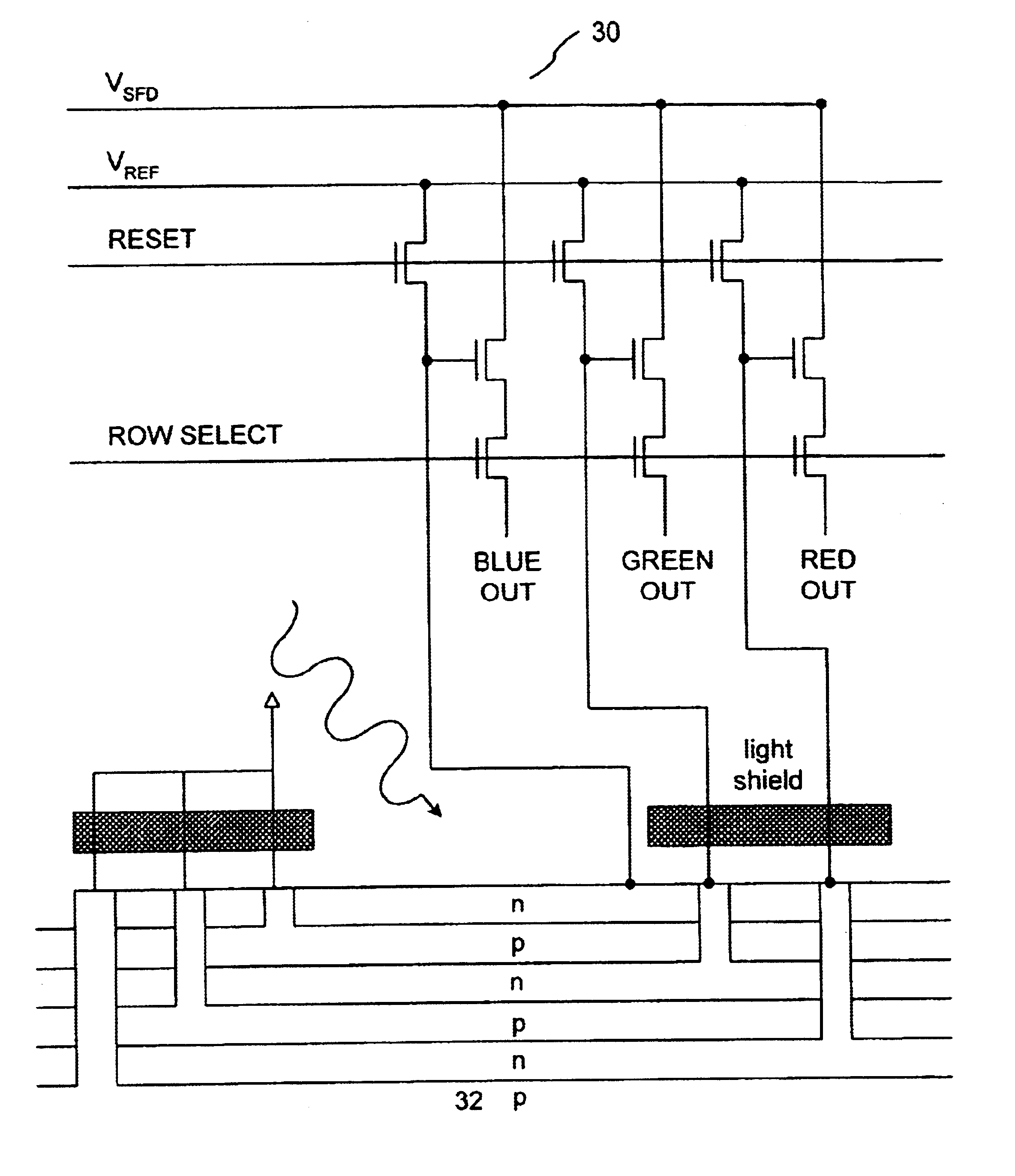
FIG. 2A illustrates an illustrative and non-limiting example of a color detector group that may be used to practice the present invention. Color detector group 30 is a six-layer structure that is shown schematically in cross-sectional view fabricated on p-type semiconductor substrate 32. This type of vertical color filter detector group has three n-type regions, isolated vertically by p-regions that are all connected to the substrate potential.

The blue, green, and red photodiode sensors are formed by the junctions between the n-type and p-type regions, and are disposed at different depths beneath the surface of the semiconductor structure. In comparison to the structure of FIG. 1., the addition of the e...


PUM


Abstract

A vertical color detector group according to the present invention is formed on a semiconductor substrate and includes layers for collecting photons of different wavelength bands. The color detector group can be programmed to perform dynamic switching between sub-sampled color data and full measured color readout. The color detector group can also be configured in a portion of an array to emulate color filter array patterns, and programmed to dynamically alter the degree to which color information is sub-sampled. The programmable color detector groups can allow for switching between different levels of quality and resolution, allowing for selection of an optimal pattern based on image content or lighting conditions. By combining the color detector group of the present invention with conventional color filters, color filter arrays of more than three colors can be constructed.

Description

BACKGROUND OF THE INVENTION1. Field of the InventionThe present invention relates to active pixel image sensors. More particularly, the present invention relates to full-color detector groups and arrays that use semiconductor material to chromatically filter light vertically and sense multiple wavelength bands at each cell or pixel location in an image sensor. The present invention also relates to such color detector groups configured in arrays and combined with circuitry so as to permit operation in various color subsampling modes as well as in full-color readout modes2. The Prior ArtMOS active pixel sensors are known in the art. Multiple wavelength active pixel sensors are also known in the art. One type of multiple wavelength active pixel sensor employs red, green, and blue sensors disposed horizontally in a pattern at or near the semiconductor surface. Color overlay filters are employed to produce the color selectivity between the red, green, and blue sensors. Such sensors have ...

Claims


Application Information

Patent Timeline
IPC IPC(8): H01L27/146
CPCH01L27/14647H01L27/14621
Inventor TURNER, RICHARD M.LYON, RICHARD F.GUTTOSCH, RUDOLPH J.MERRILL, RICHARD B.
Owner FOVEON
Learn More