
Quantum dot tunable external cavity laser (QD-TEC laser)

a laser and external cavity technology, applied in the field of photonics, can solve the problems of lasers with major limitations, limit the usefulness of semiconductor laser diodes based on quantum wells,

Inactive Publication Date: 2005-03-01
NAT RES COUNCIL OF CANADA
View PDF2 Cites 13 Cited by
  • Summary
  • Abstract
  • Description
  • Claims
  • Application Information

AI Technical Summary

Benefits of technology

Unlike the density-of-state of bulk material and of quantum wells, the electronic configuration of low-dimensional nano-structures, herein defined as quantum wires (one- or quasi-one dimensional structures) or quantum dots (zero or quasi-zero dimensional structures), will allow the saturation of their reduced density-of-states over a wide range of energies because the total number of available states is orders of magnitude smaller than for quantum wells. This will permit the production of population inversions and lasing over wide range of wavelengths. Also, it is possible to produce Self-Assembled Quantum Dots (QD) by epitaxy using highly strained semiconductors, and to have good control over their zero-dimensional density-of-state. Such quantum dots can be grown in a laser diode configuration with conventional techniques, and the carriers will be injected electrically in the QD laser diode. To obtain the tunability in such a QD laser diode having a wide gain spectrum, an external cavity is used. The resulting QD tunable external cavity (QD-TEC) laser retains the efficiency and convenience of conventional semiconductor laser diodes, and yet is tunable over hundreds of nanometers by choosing the low-dimensional electronic structure of the QD and the optical properties of the external cavity.
The QD laser diode preferably comprises multiple layers of semiconductor materials including a least one quantum dot layer in an active region between an electron emitter layer, allowing the injection of electrons towards the quantum dots, and a hole emitter layer, allowing the injection of holes towards the quantum dots. The composition and doping of the materials is chosen so that the relative optical constants, bandgaps, and conductivity of the layers establish an effective guiding of the optical modes in a cavity formed perpendicular to the plane of the layers, as well as efficient carrier injection when an electric field is applied with the proper forward-bias polarity.
The active region is preferably not doped to minimize loses of the guided optical modes. Intermediate layers with chosen bandgap and doping can also be introduced between the active region and the emitter layers to tailor the optical guiding and the optical and electrical properties of the laser diode. The current injection and the optical mode guided in the QD laser diode material are preferably confined laterally to tailor the electrical, thermal, and optical characteristic of the QD-TEC laser. The current injection in the QD laser diode material might preferably be confined longitudinally to tailor the electrical, thermal, and optical characteristic of the QD-TEC laser. The longitudinal confinement of the optical mode guided in the QD laser diode material is preferably adjusted by changing the reflectivity of a front and a back facet individually to tailor the electrical, thermal, and optical characteristic of the QD-TEC laser. It might be preferable to regulate the temperature and / or remove excess heat generated by the operation of the QD laser diode with the help of a temperature regulating device.
In another aspect the invention provides a method of producing low-dimensionality laser diodes having an adjustable gain spectrum based on a quantum material with low-dimensional density-of-states which relies on self-assembled quantum dots obtained by spontaneous island formation during epitaxy of highly strained semiconductors, comprising selecting a barrier material and a quantum material such that the degree of lattice-mismatch dictates a critical thickness required to obtain spontaneous island formation, and the bandgap difference determines a possible number of confined states in conjunction with the energy spectrum of the low-dimensional states; growing some thickness of said barrier material in an active region between an electron emitting layer and a hole emitting layer on a substrate, said electron and hole emitting layers having a lattice constant close to that of said substrate; depositing, at a specified growth rate, said quantum material at a temperature which will produce quantum dots having the appropriate size and shape to obtain said low-dimensionality density-of-states; ceasing the growth of said quantum material after the desired number of quantum dots per unit area is reached; waiting a specified amount of time to allow for the self-assembling growth to form the quantum dots in shapes and sizes which will give said low-dimensionality density-of-states; and growing some thickness of said barrier material to cover the quantum dots and return to a planar growth front at a substrate temperature which may be varied during the growth and which will optimize the quality of the quantum dots.

Problems solved by technology

This limits the usefulness of semiconductor laser diodes based on quantum wells because the 2-dimensional density-of-states of the electronic structure results in a gain spectrum which can be tuned at most by tens of nanometers using external cavities, or using integrated tuning elements.
These lasers have major limitations because they are not compact and are very inefficient since they have to be aligned and optically pumped with another powerful laser operated at shorter wavelengths.

Method used


Image

  • Quantum dot tunable external cavity laser (QD-TEC laser)
  • Quantum dot tunable external cavity laser (QD-TEC laser)
  • Quantum dot tunable external cavity laser (QD-TEC laser)

Examples


Embodiment Construction

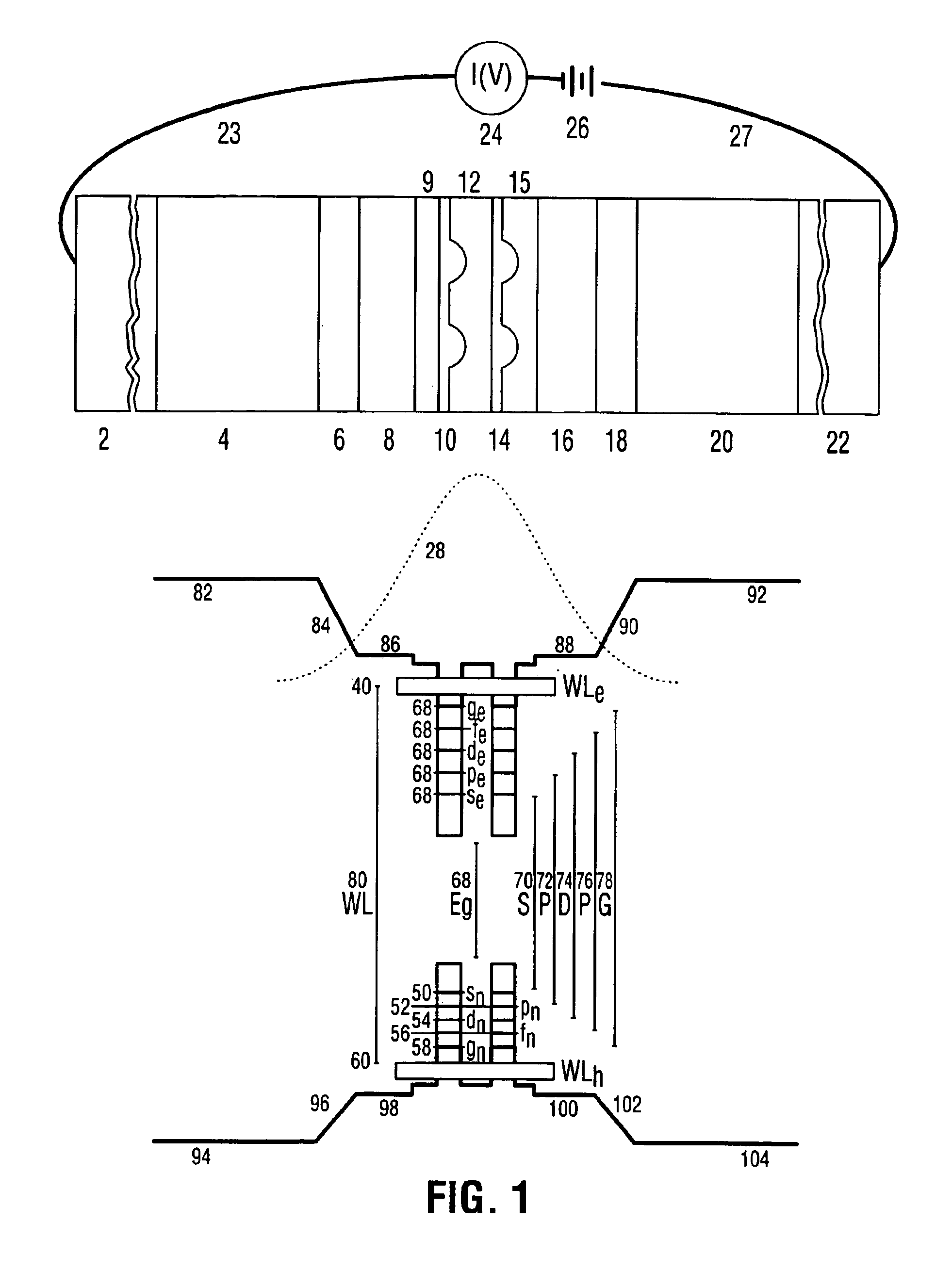
FIG. 1 shows a schematic for the quantum dot laser diode portion of the QD-TEC laser in accordance with the invention. Such a diode comprises multiple layers of semiconductor materials which are depicted in the upper part of FIG. 1, together with the corresponding energy band diagram shown in the lower part of FIG. 1. In the band diagram, the vertical direction represents the energy of the carriers in the structure, and the horizontal direction represents the position of the carriers within the laser structure. The layers are very thin; for instance in a preferred form of the device, the thickness of a quantum dot together with the wetting layer which forms below the quantum dots 10, 14 is about 4.5 nanometers or smaller. Hence, it is necessary to provide a substrate to grow the layers and to give structural integrity to the device. The substrate can be electrically conducting or insulating, and will typically have a thickness between 0.1 and 1 mm. The substrate will preferably be c...


PUM


Abstract

A laser system includes a laser diode with a low dimensional nanostructure, such as quantum dots or quantum wires, for emitting light over a wide range of wavelengths. An external cavity is used to generate laser light at a wavelength selected by a wavelength-selective element. The system provides a compact and efficient laser tunable over a wide range of wavelengths.

Description

FIELD OF THE INVENTIONThe present invention relates to the field of photonics, and more particularly to low-dimensionality semiconductor laser devices capable of emitting different frequencies.BACKGROUND OF THE INVENTIONPresently, very efficient and compact laser sources can be obtained using semiconductor laser diodes based on 2-dimensional quantum well(s) in their active gain region. Such state-of-the-art semiconductor laser diodes can produce hundreds of milliwatts of laser light emitted over a narrow range of wavelengths of a few nanometers (nm) or smaller. Typically, to obtain a different wavelength, a distinct laser diode must be fabricated with the appropriate quantum well(s) in its active region. For several applications, a wide range of wavelengths are necessary. This limits the usefulness of semiconductor laser diodes based on quantum wells because the 2-dimensional density-of-states of the electronic structure results in a gain spectrum which can be tuned at most by tens ...

Claims


Application Information

Patent Timeline
Patent Type & Authority Patents(United States)
IPC IPC(8): H01S5/00H01S5/14H01S5/34
CPCB82Y20/00H01S5/141Y10S977/951H01S5/3412Y10S438/933H01S5/143
Inventor FAFARD, SIMON
Owner NAT RES COUNCIL OF CANADA
Learn More