
Lid assembly for a processing system to facilitate sequential deposition techniques

a processing system and sequential deposition technology, applied in chemical vapor deposition coating, coating, metallic material coating process, etc., can solve the problems of affecting the deposition rate of the liquid in the chamber, the relatively small volume of gas utilized in each pulse is problematic, and the deposition rate is much lower than typical cvd techniques, so as to achieve the effect of improving the deposition rate and controlling the fluid

Inactive Publication Date: 2005-04-12
APPLIED MATERIALS INC
View PDF442 Cites 593 Cited by
  • Summary
  • Abstract
  • Description
  • Claims
  • Application Information

AI Technical Summary

Benefits of technology

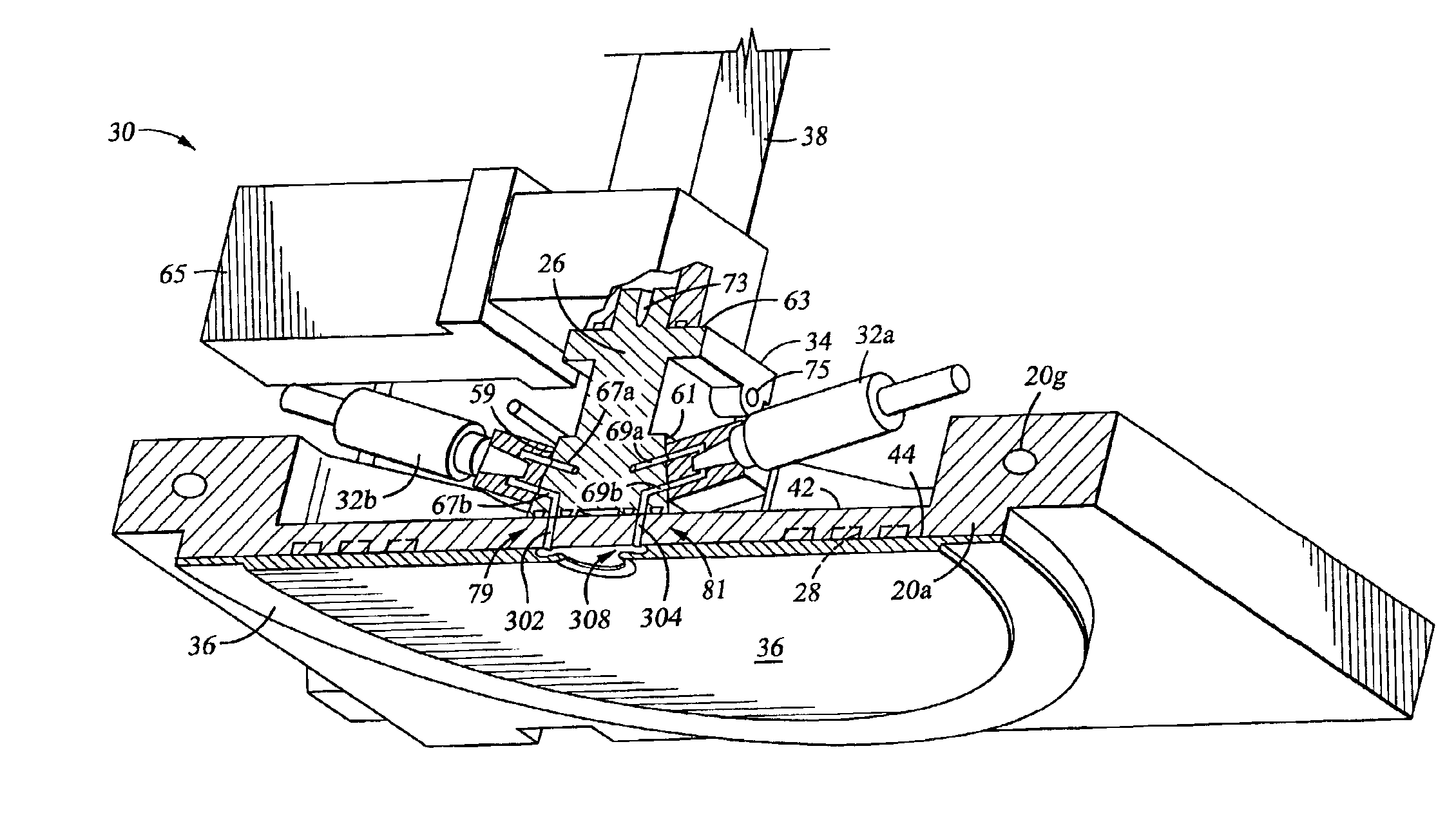
Provided is a lid assembly for a semiconductor system, an exemplary embodiment of which includes a support having opposed first and second surfaces, with a valve coupled to the first surface. A baffle plate is mounted to the second surface. The valve is coupled to the support to direct a flow of fluid along a path in an original direction and at an injection velocity. The baffle plate is disposed in the path to disperse the flow of fluid in a plane extending transversely to the original direction. The proximity of the valve to the baffle plate allows enhanced rate and control of fluid disposed through the lid assembly.

Problems solved by technology

These requirements become more critical as substrate size increases, creating a need for more complexity in chamber design and fluid flow technique to maintain adequate uniformity.
The control over the relatively small volume of gas utilized in each pulse is problematic.
Consequently, ALD techniques result in a deposition rate that is much lower than typical CVD techniques.

Method used


Image

  • Lid assembly for a processing system to facilitate sequential deposition techniques
  • Lid assembly for a processing system to facilitate sequential deposition techniques
  • Lid assembly for a processing system to facilitate sequential deposition techniques

Examples


Embodiment Construction

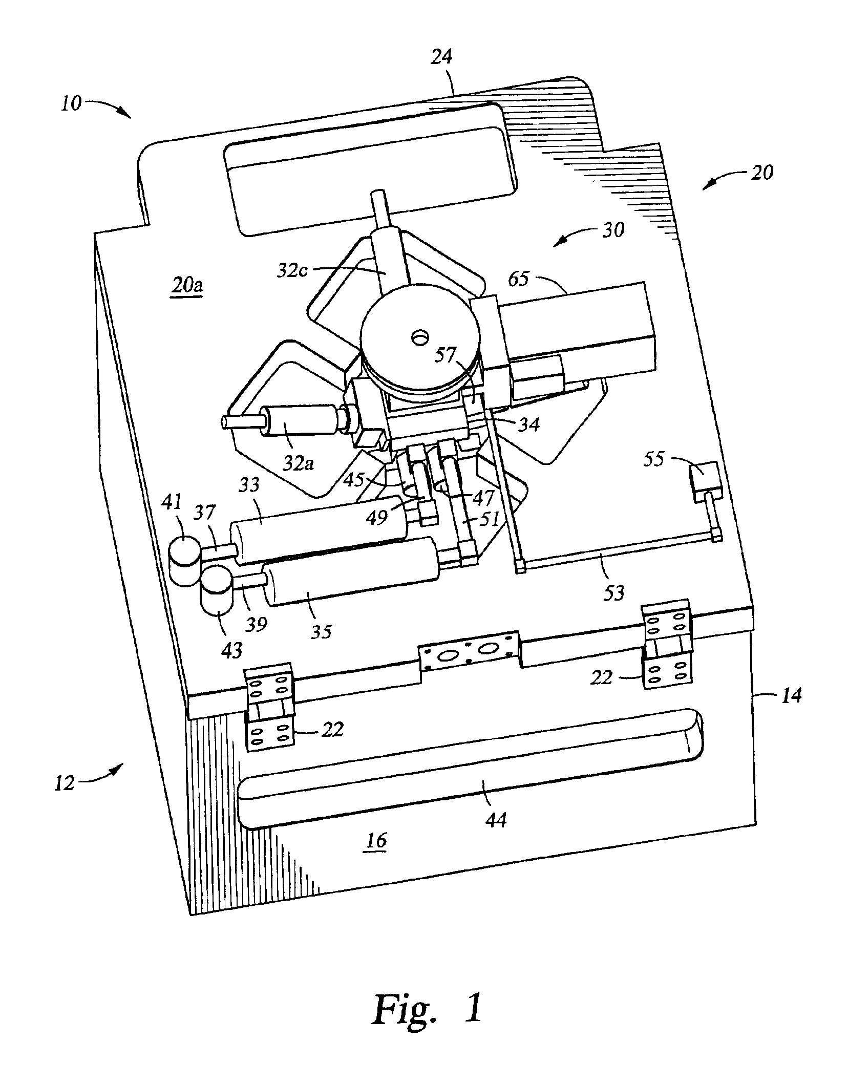
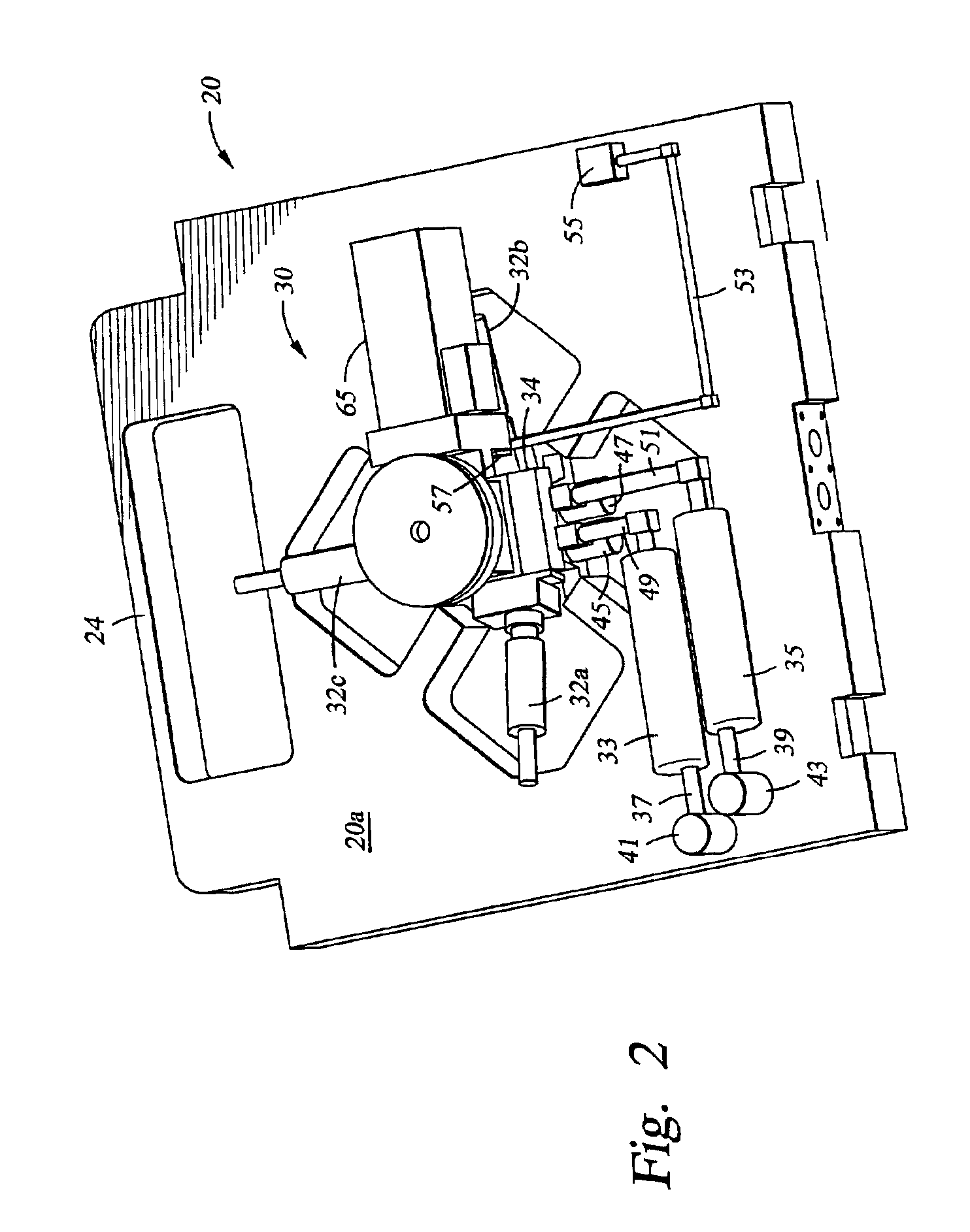
Referring to FIG. 1, a semiconductor processing system 10 in accordance with one embodiment of the present invention includes an enclosure assembly 12 formed from a process-compatible material, such as aluminum or anodized aluminum. The enclosure assembly 12 includes a housing 14, defining a processing chamber 16 with an opening 44 selectively covered and a vacuum lid assembly 20. The vacuum lid assembly 20 is pivotally coupled to the housing 14 via hinges 22. A handle 24 is attached to the vacuum lid assembly 20 opposite the hinges 22. The handle 24 facilitates moving the vacuum lid assembly 20 between opened and closed positions. In the opened position, the interior of the chamber 16 is exposed. In the closed position shown in FIG. 1, the vacuum lid assembly 20 covers the chamber 16 forming a fluid-tight seal with the housing 14. In this manner, a vacuum formed in the processing chamber 16 is maintained as the vacuum lid assembly 20 seals against the housing 14.

To facilitate acces...


PUM

PropertyMeasurementUnit
pressureaaaaaaaaaa
contact areaaaaaaaaaaa
common elevationaaaaaaaaaa

Abstract

A lid assembly for a semiconductor processing system is provided. The lid assembly generally includes a lid having a gas manifold mounted on a first side and a baffle plate mounted on a second side. The gas manifold is configured to deliver a plurality of gases to a plenum defined between the baffle plate and the lid. The gases are mixed within a recess formed in the baffle plate before exiting into the processing system through a singular passage.

Description

BACKGROUND OF THE INVENTION1. Field of the InventionThis invention relates to semiconductor processing. More particularly, this invention relates to a processing system and method of distributing fluid therein to facilitate sequential deposition of films on a substrate.2. Description of the Related ArtThe semiconductor processing industry continues to strive for larger production yields while increasing the uniformity of layers deposited on substrates having increasingly larger surface areas. These same factors in combination with new materials also provide higher integration of circuits per unit area of the substrate. As circuit integration increases, the need for greater uniformity and process control regarding layer thickness rises. As a result, various technologies have been developed to deposit layers on substrates in a cost-effective manner, while maintaining control over the characteristics of the layer. Chemical Vapor Deposition (CVD) is a common deposition process employed ...

Claims


Application Information

Patent Timeline
Patent Type & Authority Patents(United States)
IPC IPC(8): C23C16/455H01L21/00C23C16/44
CPCC23C16/45512C23C16/45544C23C16/50C23C16/455H01L21/67017C23C16/45525C23C16/45538C23C16/45561
Inventor TZU, GWO-CHUANUMOTOY, SALVADOR P.
Owner APPLIED MATERIALS INC
Learn More