CMOS transistor having different PMOS and NMOS gate electrode structures and method of fabrication thereof
- Summary
- Abstract
- Description
- Claims
- Application Information
AI Technical Summary
Benefits of technology
Problems solved by technology
Method used
Image

Examples
Embodiment Construction
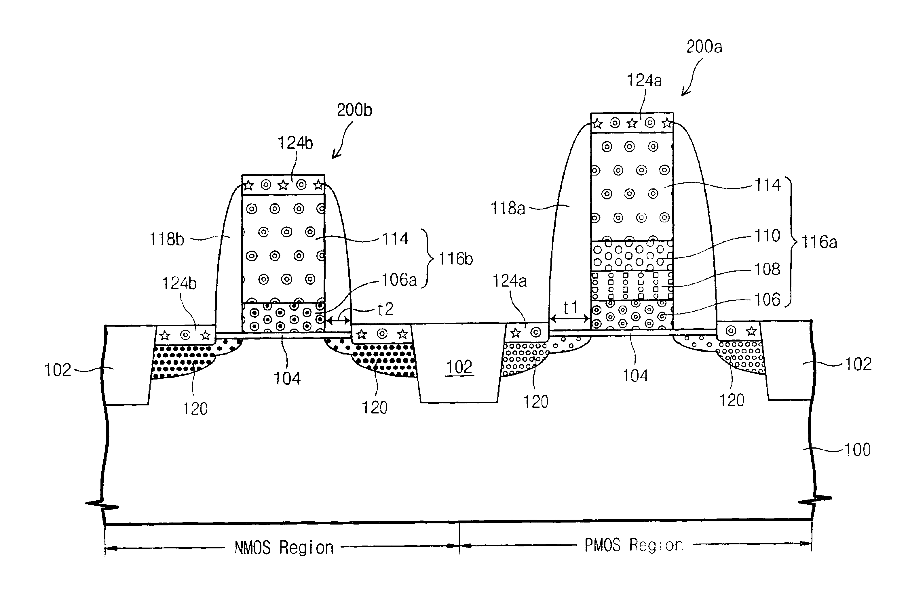
First, a structure of a semiconductor device according to the present invention will now be described with reference to FIG. 12.
As illustrated in FIG. 12, a semiconductor device includes a PMOS transistor 200a and an NMOS transistor 200b formed on a semiconductor substrate 100. The PMOS and NMOS transistors are electrically isolated by a device isolation region 102. The PMOS transistor 200a has a stacked gate electrode 116a and source / drain regions 120. A gate insulating layer 104 is interposed between the semiconductor substrate 100 and the stacked gate electrode 116a. The source / drain 120 is formed in a semiconductor substrate adjacent to opposite sides of the stacked gate electrode 116a. The NMOS transistor also has a stacked gate electrode 116b and source / drain 120 regions. A gate insulating layer 104 is interposed between the semiconductor substrate 100 and the stacked gate electrode 116b. The source / drain 120 is formed in a semiconductor substrate adjacent opposite sides of th...
PUM
 Abstract
Description
Claims
Application Information
 - R&D
- Intellectual Property
- Life Sciences
- Materials
- Tech Scout
- Unparalleled Data Quality
- Higher Quality Content
- 60% Fewer Hallucinations
Browse by: Latest US Patents, China's latest patents, Technical Efficacy Thesaurus, Application Domain, Technology Topic, Popular Technical Reports.
© 2025 PatSnap. All rights reserved.Legal|Privacy policy|Modern Slavery Act Transparency Statement|Sitemap|About US| Contact US: help@patsnap.com