
Interposer capacitor built on silicon wafer and joined to a ceramic substrate

a technology of silicon wafer and ceramic substrate, which is applied in the direction of semiconductor devices, electrical equipment, semiconductor/solid-state device details, etc., can solve the problems of increasing complexity and size increasing the area required for interconnection, and reducing the complexity of circuit (ic) chips

Inactive Publication Date: 2004-09-14
GLOBALFOUNDRIES US INC
View PDF11 Cites 31 Cited by
  • Summary
  • Abstract
  • Description
  • Claims
  • Application Information

AI Technical Summary

Benefits of technology

The present invention provides an interposer with a silicon / silicon oxide substrate, on which is formed a high performance thin film dielectric capacitor that can connect integrated circuit chips to a ceramic substrate. This interposer helps to decrease the distance between IC chips and the complexity of interconnections, which is important for high-speed devices. The interposer includes metallized vias that connect power, ground, and signals between the integrated circuit and the ceramic substrate. The thin film dielectric capacitor is made of platinum electrodes and a dielectric composed of high-K titanates or other high-K dielectric materials. The interposer can be fabricated using chemical-mechanical polishing and accurate endpoint detection. The invention helps to improve the efficiency and reliability of multichip modules and reduce the size of printed circuit boards.

Problems solved by technology

As integrated circuit (IC) chips have increased in complexity and decreased in size, the formation of interconnections between IC chips has also greatly increased in complexity.
However, when a device requires a large number of IC chips, individually packaging and mounting each IC chip greatly increases the printed circuit board area required to interconnect all the IC chips.
The former approach uses valuable real estate on the surface of the ceramic substrate and does not place the discrete capacitor in close proximity to the IC chip, while the latter approach increases the complexity of the ceramic substrate and thus, decreases yields.
This is particularly important because the thin film dielectric capacitor may be one of the most likely components to be defective, due to the close spacing of the plate electrodes and the possibility of pin-hole defects or surface irregularities causing electrical shorts or leakage in the dielectric layer between the plate electrodes.

Method used


Image

  • Interposer capacitor built on silicon wafer and joined to a ceramic substrate
  • Interposer capacitor built on silicon wafer and joined to a ceramic substrate
  • Interposer capacitor built on silicon wafer and joined to a ceramic substrate

Examples


Embodiment Construction

Referring to FIGS. 1-7, the device and method of the present invention for various exemplary embodiments is described below.

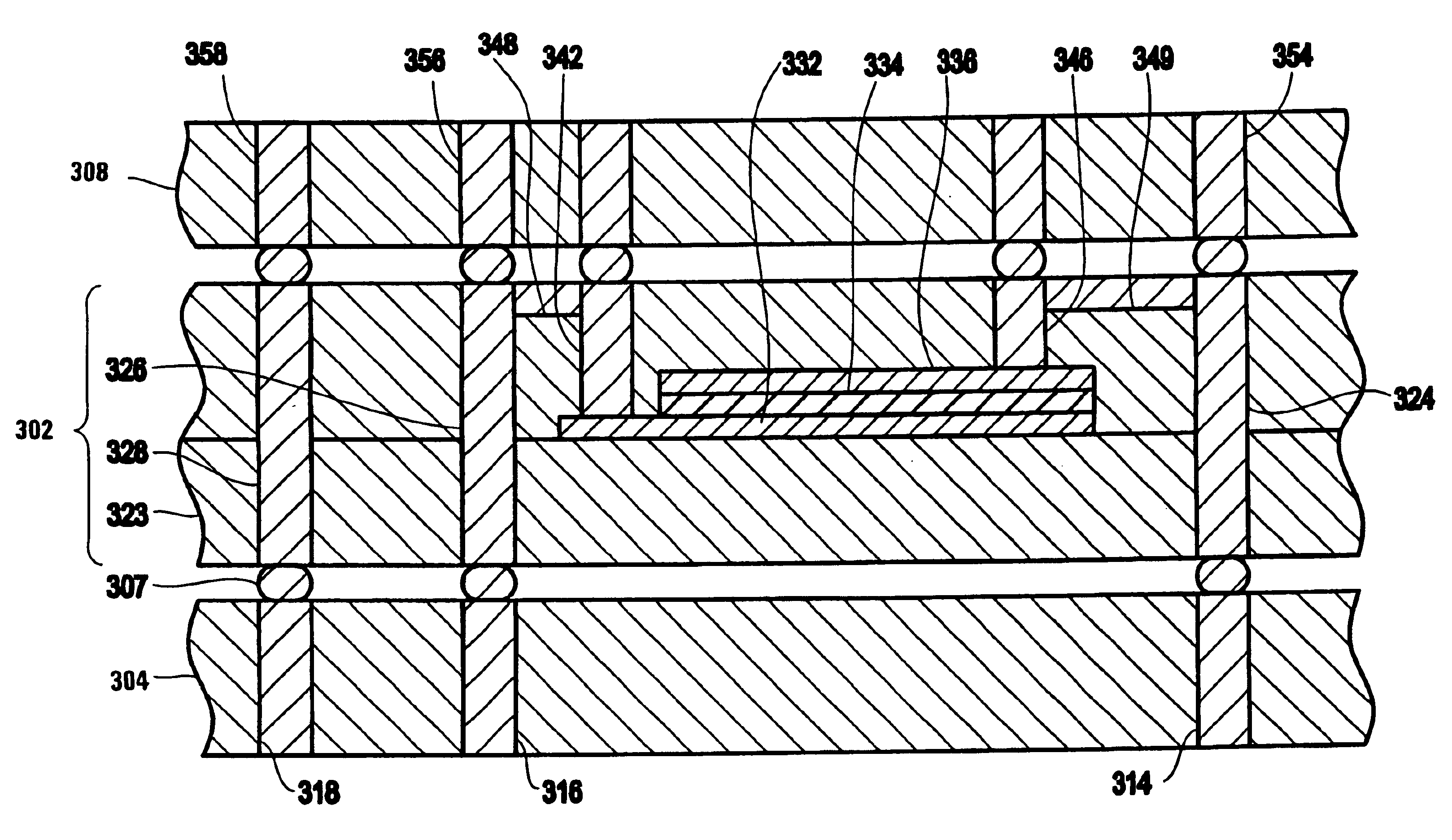
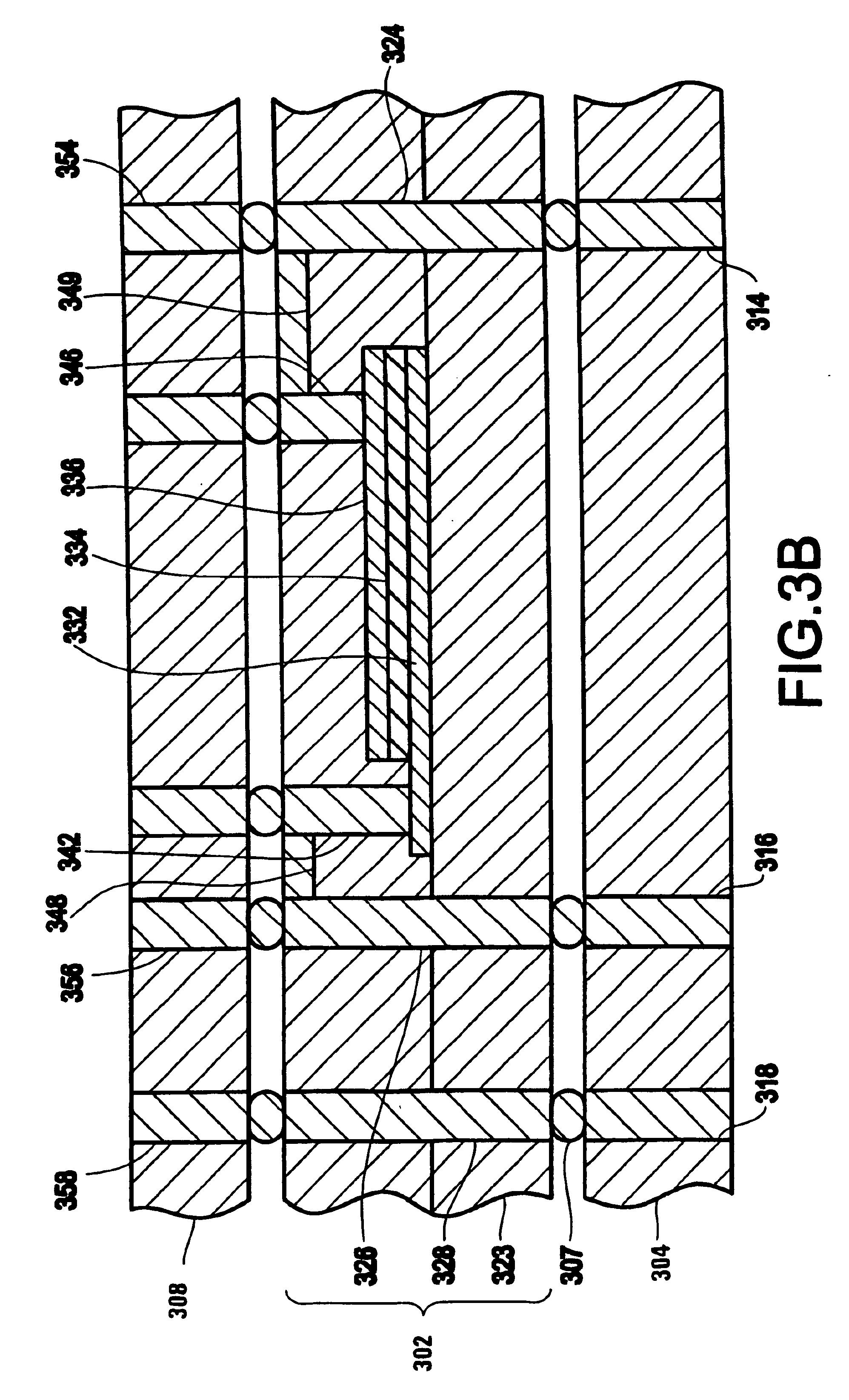
Generally, the present invention takes advantage of fabricating a thin film dielectric capacitor on a silicon / silicon oxide substrate interposer having an extremely high quality surface. The interposer may include through vias that transfer power, ground and signals from, for example, an underlying ceramic substrate to an overlying IC chip or wafer, vias that connect electrodes of the thin film dielectric capacitor to the IC chip or wafer, and interconnections among the through vias transferring power and ground to the vias connecting the electrodes of the thin film capacitor. One side of the interposer may connect to the IC chip, while the other side of the interposer may connect to the ceramic substrate. In this manner, surface defects of the ceramic substrate will not impact yields of the thin film dielectric capacitor.

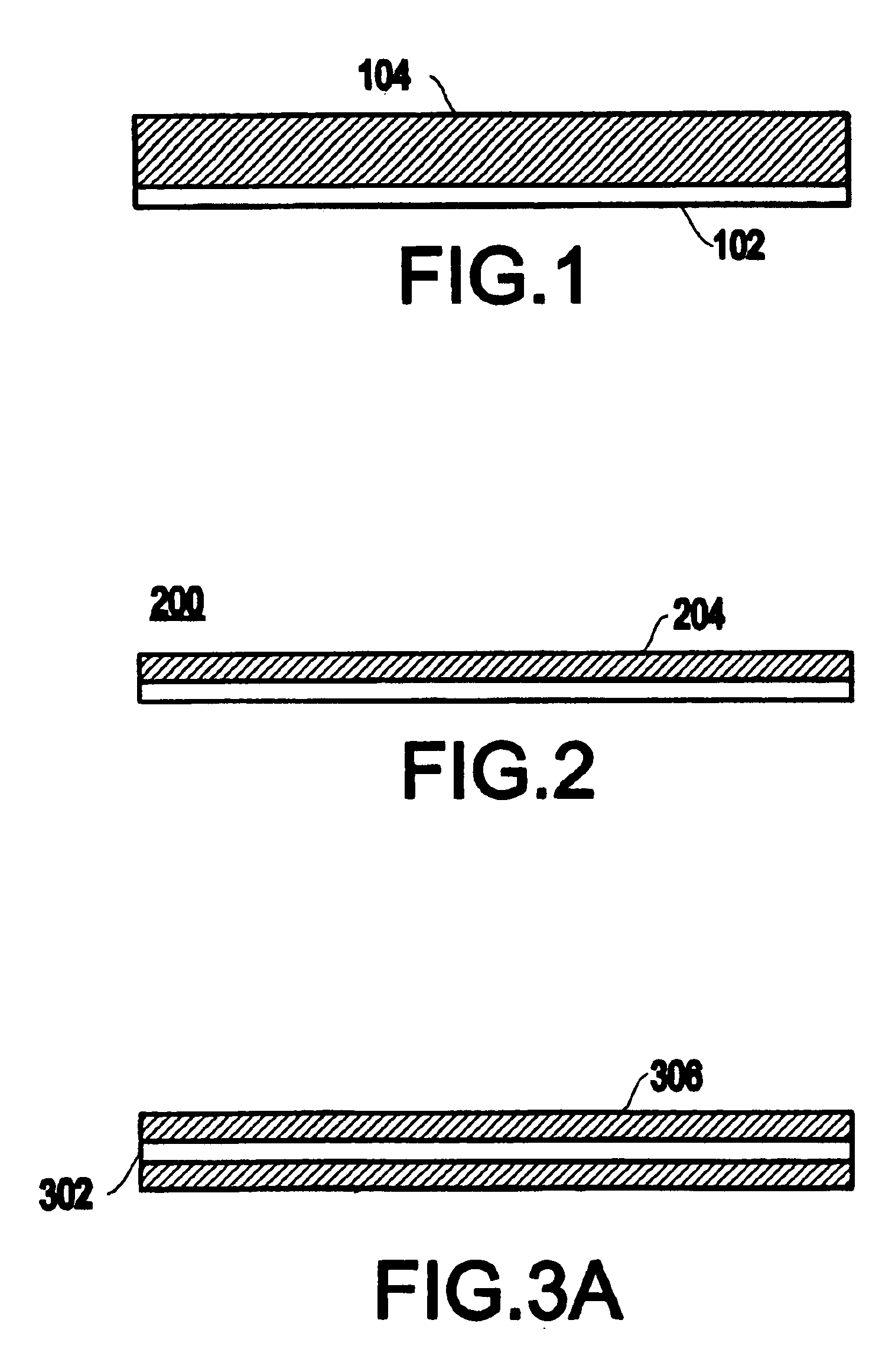
Referring to FIG. 1, an oxide layer 102...


PUM

PropertyMeasurementUnit
thicknessaaaaaaaaaa
thicknessaaaaaaaaaa
thicknessaaaaaaaaaa

Abstract

An interposer, located between an integrated circuit having power, ground and signal connections and a ceramic substrate having power, ground and signal connections, that includes an oxide layer formed on a polished surface of a silicon substrate, a thin film dielectric capacitor formed on the oxide layer, a plurality of metallized that electrically connect to either of the electrodes of the thin film dielectric capacitor, and vias than conduct power, ground and signals between a the ceramic substrate and the integrated circuit. The interposer connects the metallized vias to the integrated circuit by solder connections and also connects the vias conducting power, ground and signals from the ceramic substrate to the interposer by solder connections. The dielectric of the thin film dielectric capacitor may be selected from the group of high-K titanates, such as, barium zirconate titanate, barium strontium titanate, pure barium titanate, barium titanate modified with Pb, Nb, W, Ca, Mg, and Zn, lead titanate, lead zirconate titanate, and polycrystalline lanthanum-modified lead zirconate titanate, or other high-K dielectrics, such as, lead niobate and its derivatives, and lead tungstate and its derivatives.

Description

1. Field of the InventionThe present invention generally relates to packaging of integrated circuit devices, and is particularly related to a thin film capacitor formed on a silicon / silicon oxide substrate interposer, which is connected to a ceramic substrate and to a method of making the same.2. Description of the Related ArtAs integrated circuit (IC) chips have increased in complexity and decreased in size, the formation of interconnections between IC chips has also greatly increased in complexity. Many devices, such as computers, use a number of separate IC chips. For example, a computer may include one or more central processing units, an arithmetic processor, various controller and memory chips, input / output interface chips, etc. Conventionally, each IC chip is mounted individually in a separate package that is connected to a printed circuit board, for example, a computer "motherboard," which provides power and signal interconnections to the mounted IC chips. However, when a de...

Claims


Application Information

Patent Timeline
Patent Type & Authority Patents(United States)
IPC IPC(8): H01L23/48H01L23/498H01L23/12H01L23/32
CPCH01L23/49822H01L23/49827H01L2224/16H01L2924/00014H01L2224/0401
Inventor FAROOQ, MUKTA GHATEKNICKERBOCKER, JOHN U.REDDY, SRINIVASARITA, ROBERT ANTHONY
Owner GLOBALFOUNDRIES US INC
Learn More