
Dielectric etch chamber with expanded process window

a technology of dielectric etching and process window, which is applied in the direction of coating, chemical vapor deposition coating, coating, etc., can solve the problems of etch reaction by-products forming deposits on the exposed chamber surface, rapid shrinkage of critical dimensions, and small footprint devices

Inactive Publication Date: 2004-04-06
APPLIED MATERIALS INC
View PDF38 Cites 88 Cited by
  • Summary
  • Abstract
  • Description
  • Claims
  • Application Information

AI Technical Summary

Benefits of technology

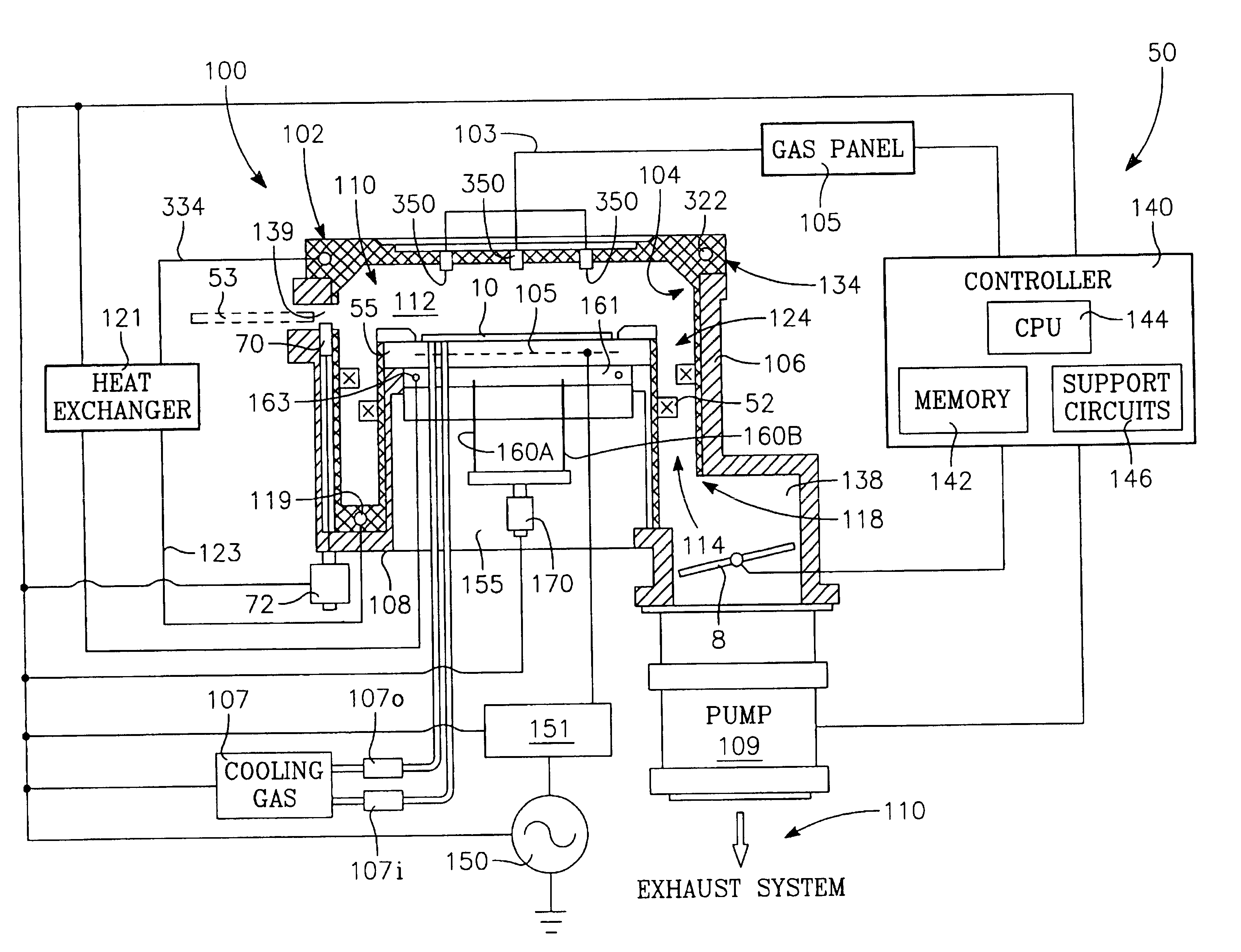
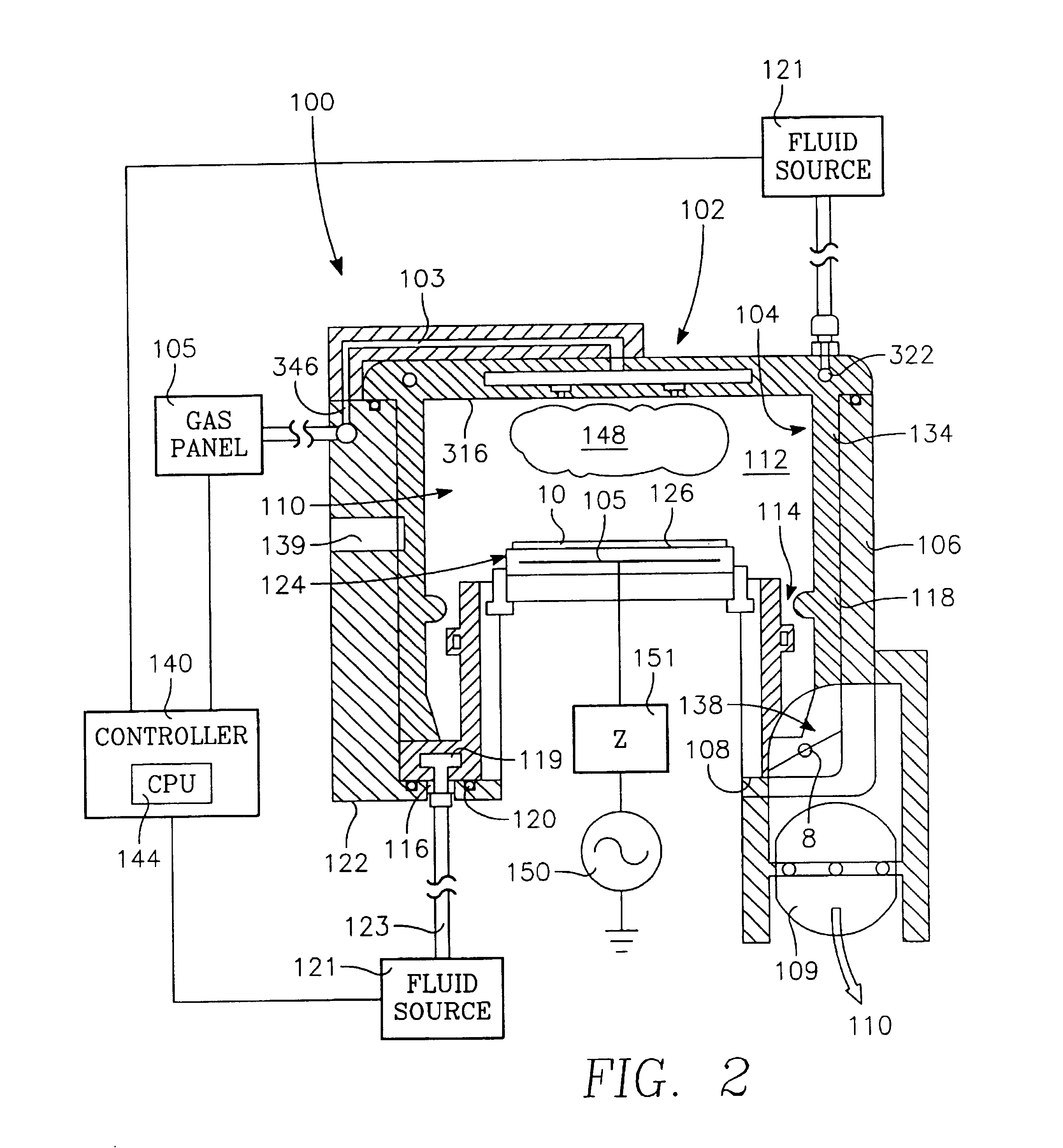
Another advantage of the present invention is the use of chamber surface topography to improve the adhesion of by products deposited on chamber surfaces. For example, in a conventional fluorocarbon based plasma etch of oxide features, polymeric byproduct formation is common. Referring to FIG. 2, for example, by-product deposition would occur on the surfaces of the two liners 118, 134 and lid 102 exposed to the plasma 148. After the deposits accumulate to a certain thickness, the deposits will begin to flake off the lid and the chamber liners, thereby contaminating the semiconductor devices being fabricated.
is the use of chamber surface topography to improve the adhesion of by products deposited on chamber surfaces. For example, in a conventional fluorocarbon based plasma etch of oxide features, polymeric byproduct formation is common. Referring to FIG. 2, for example, by-product deposition would occur on the surfaces of the two liners 118, 134 and lid 102 exposed to the plasma 148. After the deposits accumulate to a certain thickness, the deposits will begin to flake off the lid and the chamber liners, thereby contaminating the semiconductor devices being fabricated.
It is believed this aspect of the present invention further improves adhesion of reaction byproducts or other material deposited on surfaces within the process chamber that are exposed to process gases, thereby allowing the chamber to be operated for longer time intervals between cleaning such surfaces. Moreover, the improved byproduct adhesion capability promotes the use of expanded process gas compositions-including those with high rates of byproduct formation. Specifically, chamber interior surfaces such as the surface of the temperature controlled liner and lid, are fabricated with a surface contour or "texture" having topographical features--i.e., alternating protrusions and depressions (peaks and troughs)--whose width, spacing, and height dimensions are between 100 microns (0.1 mm) and 100 mm, and preferably in the range of 500 microns (0.5 mm) to 8000 microns (8 mm). In contrast, the average roughness of surfaces treated by conventional bead blasting is about 4 to 6 microns (0.15 to 0.23 mil), which is at least 16 times smaller than the features of the invention.
By "topographical feature" or "elevation feature" of the surface we mean an area whose elevation deviates from the average surface elevation. A topographical feature can be either a convex protrusion or a concave depression. The "height" of a feature is the peak-to-trough deviation in elevation. If the feature is a concave depression, the "height" of the feature is the depth of the depression.
It is believed that our textured surface improves adhesion of the deposited material for at least two reasons. One reason is that vertical contours (contours perpendicular to the average surface plane) increase compressive forces within the deposited film in a direction normal to the surface, thereby resisting cracking of the film due to thermal expansion and contraction. A second reason is that a textured surface has a greater surface area for the material to bond to than a flat surface.
The surface area increases in proportion to the depth of the depressions or the height of the protrusions. While increasing the height dimension in order to increase the surface area by improves adhesion of deposited material, increasing the height beyond a certain value can become disadvantageous. First, an excessive height dimension can make the textured surface harder to clean. Secondly, if the textured surface is a thin, removable chamber lid or liner rather than a comparatively thick chamber wall, an excessive height dimension can reduce the strength and rigidity of the lid or liner, making it more susceptible to accidental damage.

Problems solved by technology

One challenge facing all forms of semiconductor processing is the industry wide progression towards decreasing feature sizes resulting in rapidly shrinking critical dimensions.
Another challenge facing semiconductor processing is the trend towards smaller footprint devices.
However, some etch reaction by-products form deposits on exposed chamber surfaces and on surfaces of the etched structure.
Conventional etch chambers lack appropriate thermal management techniques to reduce thermally induced stresses between accumulated deposits and chamber components.
Eventually, the stresses can cause the deposits to crack, consequently releasing particles into the chamber environment.
These film particles may impinge upon the wafer surface, typically creating a defect in the circuit structure on the wafer.
As feature sizes decrease, however, sidewall profile control becomes increasingly more difficult and possibly unfeasible using conventional plasma etch chambers.

Method used


Image

  • Dielectric etch chamber with expanded process window
  • Dielectric etch chamber with expanded process window
  • Dielectric etch chamber with expanded process window

Examples


example 1

Pyramid Depressions in Aluminum Nitride Roof

We fabricated a chamber roof (gas distribution plate) as a circular disk of aluminum nitride ceramic, 0.5 inch (13 mm) thick, in which we divided the lower circular surface of the roof (the surface exposed to the chamber interior) into four quadrants, with four different surface textures fabricated in the four quadrants. The first quadrant was smooth, and the second quadrant was bead blasted with silicon carbide particles.

The third and fourth quadrants both had the pyramid texture 60a shown in FIG. 15, with bead blasting subsequently applied to the fourth quadrant but not the third. The dimensions of the pyramid features were: angle .theta.=45.degree., height H=0.6 mm, width W=1.5 mm, spacing S=0.6 mm. We calculate that the third quadrant had a surface area 30% greater than that of the first quadrant due to its pyramid texture.

We expect that a pattern of square depressions or protrusions 60 as shown in FIG. 14 would be preferable to the py...

example 2

Different Pyramid Dimensions in Aluminum Nitride Roof

A second aluminum nitride roof (gas distribution plate) was fabricated as described for Example 1. The four quadrants were textured with pyramids having different dimensions, as summarized in Table 1. In the first quadrant, the pyramid dimensions were identical to those of quadrant 3 of Example 1. In the other three quadrants, the height H of the pyramid depressions was increased to 1.1 mm. In quadrants 3 and 4, the angle .theta. of the pyramid walls relative to the horizontal surface was decreased to 30.degree.. In quadrants 2 and 4, the width W and spacing S were increased to 2.5 mm and 1.0 mm, respectively. All four quadrants exhibited no flaking of the polymer deposits.

example 3

Hemispherical Depressions in Aluminum Oxide Roof

We fabricated a roof of a 0.5 inch (13 mm) thick plate of aluminum oxide (alumina) ceramic. Alumina has a much lower thermal conductivity than aluminum nitride, but it has the advantage of being readily machinable. We created the pattern of depressions shown in FIGS. 16 and 17 by drilling in the alumina an array of approximately hemispherical holes, or holes having an arcuate cross section, having a hole diameter W of 4 mm and a spacing S between the perimeters of adjacent holes of 1 mm. We tested two prototypes in which the depth of the holes (the topographical feature height H) were 1 mm and 2 mm, respectively. Both prototypes exhibited no flaking of the polymer deposits.


PUM

PropertyMeasurementUnit
residency timeaaaaaaaaaa
feature sizesaaaaaaaaaa

Abstract

A capacitively coupled reactor for plasma etch processing of substrates at subatmospheric pressures includes a chamber body defining a processing volume, a lid provided upon the chamber body, the lid being a first electrode, a substrate support provided in the processing volume and comprising a second electrode, a radio frequency source coupled at least to one of the first and second electrodes, a process gas inlet configured to deliver process gas into the processing volume, and an evacuation pump system having pumping capacity of at least 1600 liters / minute. The greater pumping capacity controls residency time of the process gases so as to regulate the degree of dissociation into more reactive species.

Description

BACKGROUND OF THE DISCLOSURE1. Field of InventionThe present invention relates generally to a semiconductor wafer processing apparatus. More specifically, the invention relates to a dielectric etch processing chamber having improved thermal and by-product management capabilities, improved control of gaseous species residence time, and an expanded process window including high flow rates and low operating pressures.2. Background of the InventionOne challenge facing all forms of semiconductor processing is the industry wide progression towards decreasing feature sizes resulting in rapidly shrinking critical dimensions. Current design rules have feature sizes of less than about 0.18 microns and feature sizes below about 0.1 microns are being developed.Another challenge facing semiconductor processing is the trend towards smaller footprint devices. One approach to achieving a smaller device footprint is to build the device structure vertically and in some devices, fabricating portions o...

Claims


Application Information

Patent Timeline
Patent Type & Authority Patents(United States)
IPC IPC(8): H01L21/60H01L21/02H01L21/687H01L21/683H01L21/00H01L21/67H01J37/32H01L21/768H01L21/70H01L21/311
CPCH01J37/32522H01L21/31116H01L21/67069H01L21/6833H01L21/6875H01L21/68757H01L21/68785H01L21/68792H01L21/76802H01L21/76807H01L21/76897H01L2924/3011
Inventor CARDUCCI, JAMES DNOORBAKHSH, HAMIDLEE, EVANS YPU, BRYAN YSHAN, HONGCHINGBJORKMAN, CLAESSALIMIAN, SIAMAKLUSCHER, PAUL EWELCH, MICHAEL D
Owner APPLIED MATERIALS INC
Learn More