
Thin-film edge field emitter device

a technology of emitter device and thin film, which is applied in the manufacture of discharge tube main electrodes, electrode systems, electric discharge tube/lamps, etc., can solve the problems of small localized vacuum electron source which emits sufficiently high current for practical applications, difficult to fabricate, and difficult to create feas

Inactive Publication Date: 2001-06-12
THE UNITED STATES OF AMERICA AS REPRESENTED BY THE SECRETARY OF THE NAVY
View PDF11 Cites 3 Cited by
  • Summary
  • Abstract
  • Description
  • Claims
  • Application Information

AI Technical Summary

Benefits of technology

It is another object of the present invention to provide a field emitter device having inherent advantages over previous electron sources, including higher emission currents, lower power requirements, less expensive fabrication costs and ease of integration with other circuitry.
It is a further object of the present invention to fabricate FEAs over a large area in a manner which is inexpensive, yet results in an equal or greater degree of precision and reproducibility when compared with other prior art processes.

Problems solved by technology

Very small localized vacuum electron sources which emit sufficiently high currents for practical applications are difficult to fabricate.
Photo emitters have similar problems with regard to low currents and current densities.
It is difficult to create FEAs which have reproducibly small radius-of-curvature field emitter tips of conducting materials.
Furthermore, it is equally difficult to gate or grid these structures where the gate-to-emitter distance is reasonably small to provide the necessary high electrostatic field at the field emitter tip with reasonably small voltages.
Practical methods generally require the use of lithography which has a number of inherent disadvantages including the high cost of the equipment needed.
Furthermore, the high degree of spatial registration required prevents parallel processing, i.e., the fabrication of a very large number of emitters at the same time in a single process.
Furthermore, large grains might result in a rough surface.
If the side-walls were not substantially parallel to the direction of etching, then material might be disadvantageously removed.

Method used


Image

  • Thin-film edge field emitter device
  • Thin-film edge field emitter device
  • Thin-film edge field emitter device

Examples


example 1

This example is shown in FIG. 18(d) and constitutes a lithium layer sandwiched between two platinum layers. It was manufactured as follows:

(1) The starting work piece consisted of a 10.times.10 array of silicon template structures 10 .mu.m in diameter and 2 .mu.m in height, spaced at 500 .mu.m apart, and centered in a 5.times.5 millimeter (mm) area on a 1.times.1 cm piece of n-type Si(100) overcoated with a 200 .ANG.layer of amorphous silicon. These cylindrical protuberances were fabricated using standard photo-lithographic methods.

(2) The sample was cleaned by 5 minute immersions in warm acetone, 10% buffered HF, H.sub.2 SO.sub.4 / H.sub.2 O.sub.2, 10% buffered HF, and 1% buffered HF. A triple-distilled water rinse was used between each step except before the last HF treatment. the work piece was then mounted on a heater on a manipulator, and placed in a vacuum chamber pumped by a liquid-nitrogen trapped diffusion pump. The base pressure was 9.times.10.sup.-8 Torr. the work piece wa...

example 2

Steps (1) and (2), the procedures were the same as above except for the following: After the sample was cleaned and treated in HF, some indium metal was melted onto the back side of the substrate with a soldering iron to provide a good conducting contact for electrical connection in the later testing stage. The vacuum chamber base pressure was 3.times.10.sub.-8 Torr. The dehydration temperature prior to film deposition was 490.degree. C. for 25 minutes. The deposition temperature was 288.degree. C.

Step (3), the procedures were the same as in step (3) above except that the deposition time for Li was 8 minutes.

Step (4), the procedures were the same as in step (4) above except that the sputtering was done at 2.0 keV starting at the beginning, for 3 hours 30 minutes.

Step (5), the procedures were the same as in step (5) above except that the ion beam assisted etching step was carried out for 15 minutes at a reduced XeF2 pressure of 0.6.times.10-5 Torr.

example 3

Steps (1) and (2), the procedures were the same as above except for the following: The dehydration temperature was 503.degree. C.

Step (3), the procedures were the same as in step (3) above except that only a Pt film was deposited for 16 minutes. Pressure and temperature conditions were the same as in Example 2.

Step (4), the same procedures were used as in Example 2 above except that the sputtering was done for 2 hours 4 minutes.

Step (5), the procedures were the same as in Example 2 above except that the etching duration was 18.0 minutes.

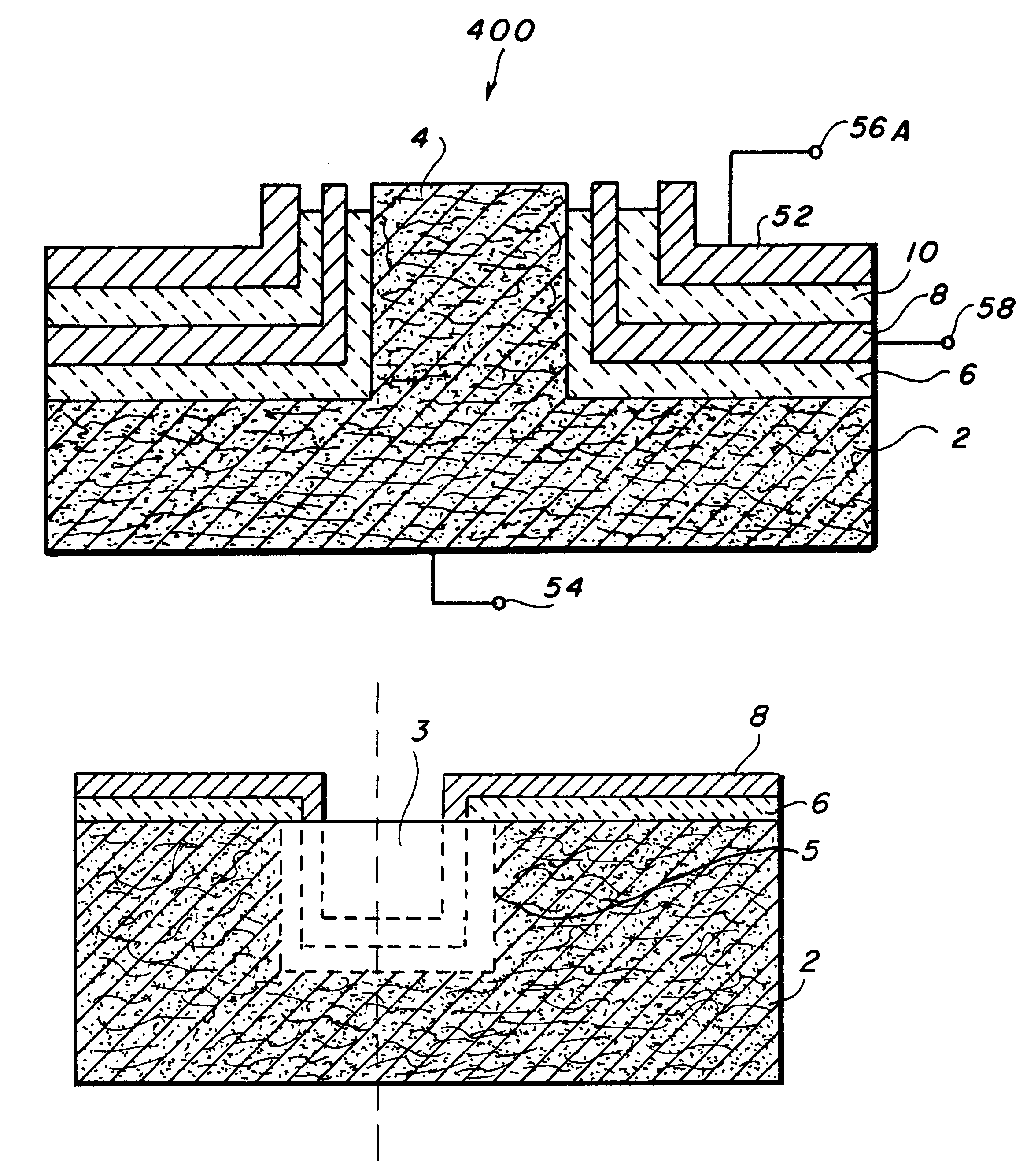
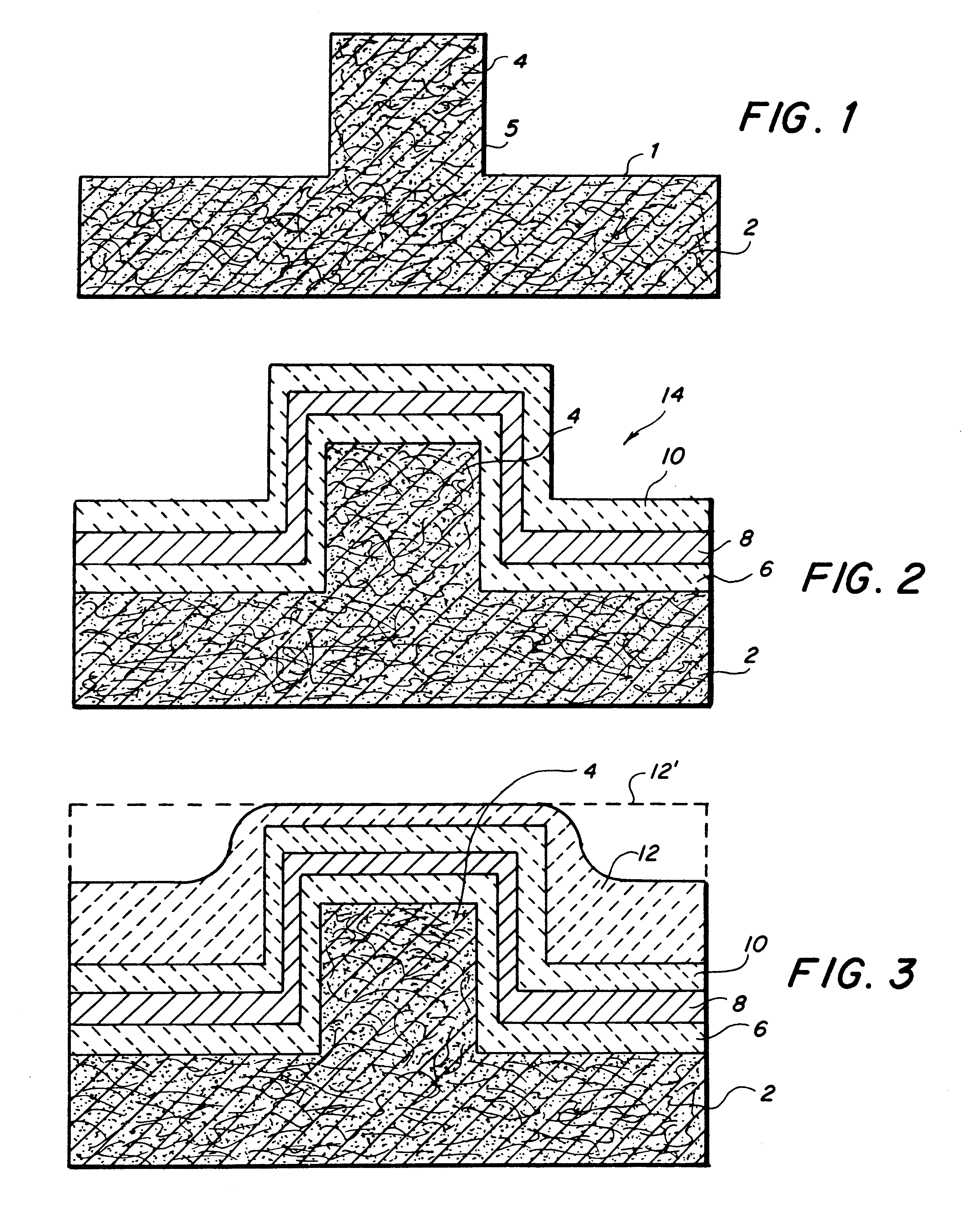
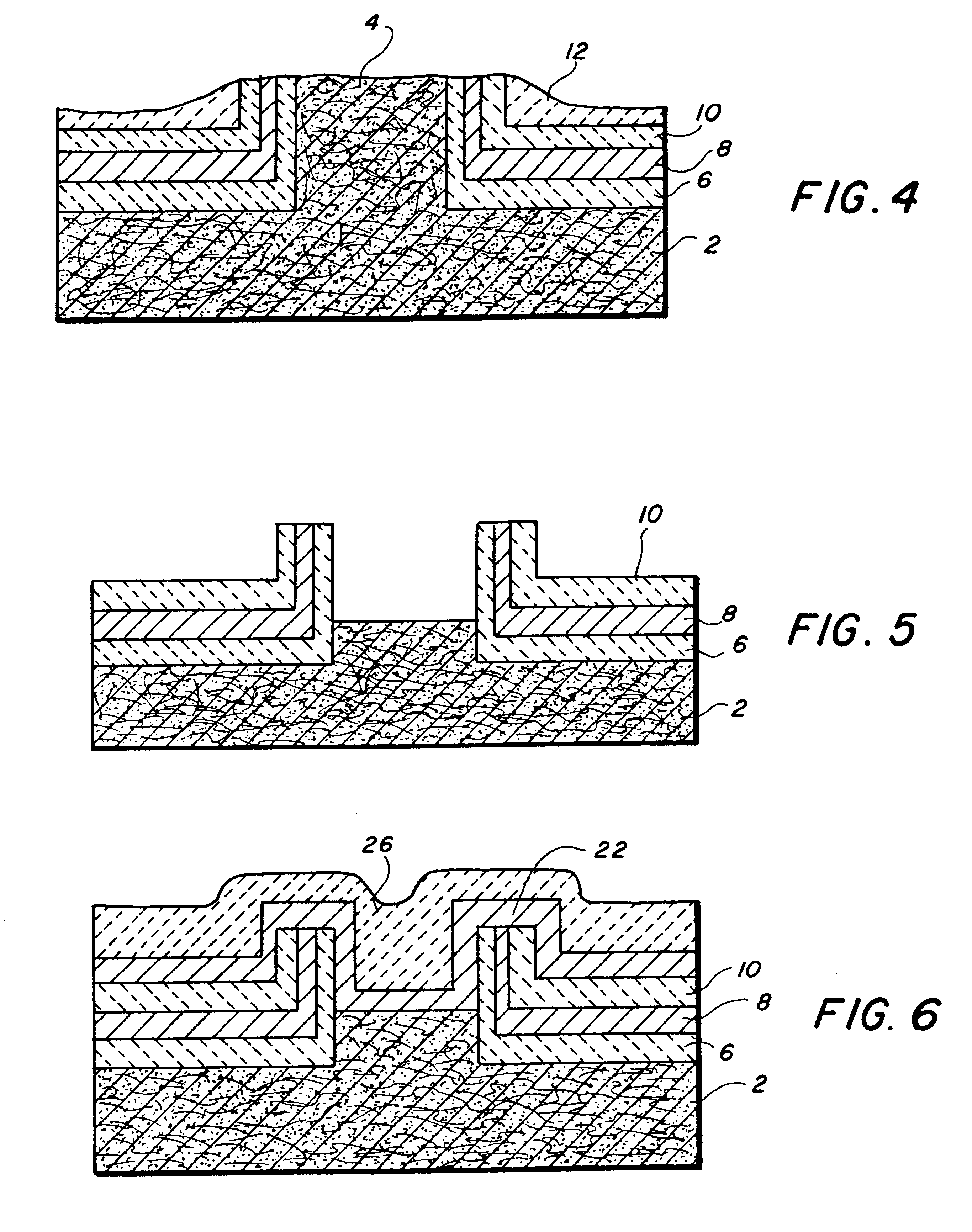
In a preferred embodiment the typical emitter structure has a shape of a hollow cylinder with nanometer (nm) linewidth wall, 2 .mu.m in height and 10 .mu.m in diameter. The cylinder wall consists of two free-standing platinum thin films sandwiching a third thin film of lower work function material. Critical material properties include very low film stress and fine grain size. The latter property allows 10-20 nm radii of curvature to be obtained. Fiel...


PUM


Abstract

A thin-film edge field emitter device includes a substrate having a first portion and having a protuberance extending from the first portion, the protuberance defining at least one side-wall, the side-wall constituting a second portion. An emitter layer is disposed on the substrate including the second portion, the emitter layer being selected from the group consisting of semiconductors and conductors and is a thin-film including a portion extending beyond the second portion and defining an exposed emitter edge. A pair of supportive layers is disposed on opposite sides of the emitter layer, the pair of supportive layers each being selected from the group consisting of semiconductors and conductors and each having a higher work function than the emitter layer.

Description

The present invention relates to ungated and gated thin-film edge field emitters capable of emitting electrons of relatively low voltage and to methods for making the same.DESCRIPTION OF THE RELATED ARTVery small localized vacuum electron sources which emit sufficiently high currents for practical applications are difficult to fabricate. This is particularly true when the sources are required to operate at reasonably low voltages. Presently available thermionic sources do not emit high current densities, but rather result in small currents being generated from small areas. In addition, thermionic sources must be heated, requiring special heating circuits and power supplies. Photo emitters have similar problems with regard to low currents and current densities.Field emitter arrays (FEAs) are naturally small structures which provide reasonably high current densities at low voltages. FEAs typically comprise an array of conical, pyramidal or cuspshaped point, edge or wedge-shaped vertic...

Claims


Application Information

Patent Timeline
IPC IPC(8): H01J1/304H01J1/30H01J9/02
CPCH01J1/3042H01J9/025H01J2201/30423H01J2201/319
Inventor HSU, DAVID S.GRAY, HENRY F.
Owner THE UNITED STATES OF AMERICA AS REPRESENTED BY THE SECRETARY OF THE NAVY
Learn More