Method of fabricating a MOS transistor with a raised source/drain extension

a technology of mos transistor and source/drain extension, which is applied in the direction of basic electric elements, electrical equipment, semiconductor devices, etc., can solve the problems that the structure and method of conventional mos transistor fabrication cannot be simply "scaled down" to produce smaller transistors for higher density integration, parasitic resistance adversely affects (reduces) the transistor drive curren

Inactive Publication Date: 2000-09-19
INTEL CORP
View PDF4 Cites 160 Cited by
  • Summary
  • Abstract
  • Description
  • Claims
  • Application Information

AI Technical Summary

Problems solved by technology

Unfortunately, the structure and method of fabrication of conventional MOS transistors cannot be simply "scaled down" to produce smaller transistors for higher density integration.
Parasitic resistance adversely effects (reduces) the transistors drive current.

Method used


Image

  • Method of fabricating a MOS transistor with a raised source/drain extension
  • Method of fabricating a MOS transistor with a raised source/drain extension
  • Method of fabricating a MOS transistor with a raised source/drain extension

Examples


Embodiment Construction

A novel transistor with a low resistance ultra shallow tip and its method of fabrication is described. In the following description numerous specific details are set forth, such as specific materials, dimensions, and processes, etc., in order to provide a thorough understanding of the present invention. It will be obvious, however, to one skilled in the art, that the invention may be practiced without these specific details. In other instances, well-known semiconductor equipment and processes have not been described in particular detail in order to avoid unnecessarily obscuring the present invention.

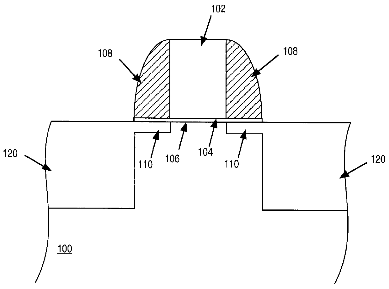
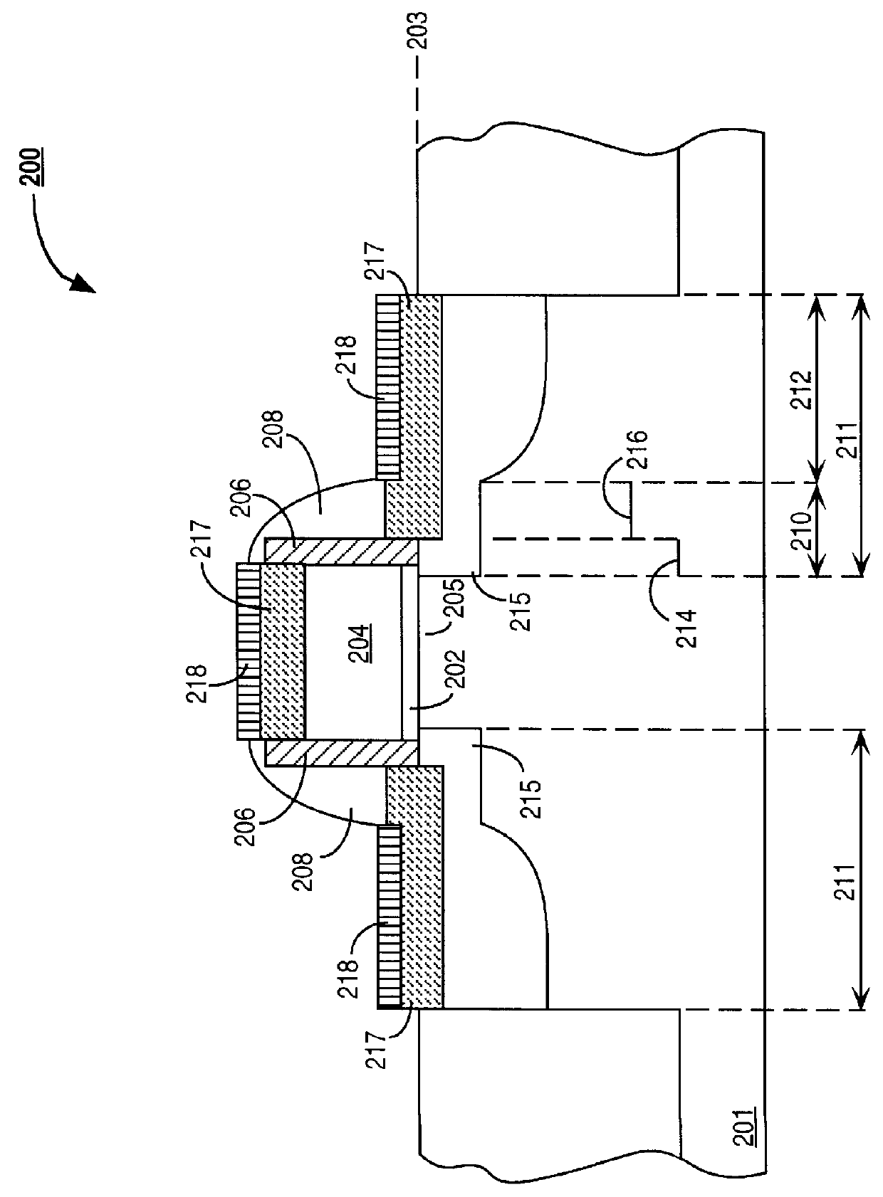
An embodiment of a novel transistor 200 with a low resistivity, ultra shallow tip in accordance with the present invention is shown in FIG. 2. Transistor 200 is formed on a silicon substrate or well 201. A gate dielectric layer 202 is formed on a surface 203 of substrate 201 and a gate electrode 204 is in turn formed on gate dielectric layer 202. A pair of thin sidewall spacers 206 are f...


PUM


Abstract

A method of forming a MOS transistor. According to the method of the present invention, a pair of source/drain contact regions are formed on opposite sides of a gate electrode. After forming the pair of source/drain contact regions, semiconductor material is deposited onto opposite sides of the gate electrode. Dopants are then diffused from the semiconductor material into the substrate beneath the gate electrode to form a pair of source/drain extensions.

Description

1. Field of the InventionThe present invention relates to the field of semiconductor integrated circuits, and more specifically, to the ultra large-scale fabrication of submicron transistors.2. Discussion of Related ArtToday literally millions of individual transistors are coupled together to form very large-scale integrated (VLSI) circuits, such as microprocessors, memories, and applications specific integrated circuits (ICs). Presently, the most advanced ICs are made up of approximately Five million transistors, such as metal oxide semiconductor (MOS) field effect transistors having gate lengths on the order of 0.35 .mu.m. In order to continue to increase the complexity and computational power of future integrated circuits, more transistors must be packed into a single IC (i.e., transistor density must increase). Thus, future ultra large-scale integrated (ULSI) circuits will require very short channel transistors with effective gate lengths less than 0.1 .mu.m. Unfortunately, the ...

Claims


Application Information

Patent Timeline
Patent Type & Authority Patents(United States)
IPC IPC(8): H01L21/225H01L21/02H01L29/49H01L21/70H01L29/66H01L29/45H01L29/40H01L21/336H01L29/417H01L29/78H01L21/8238
CPCH01L21/2254H01L21/823814H01L29/41766H01L29/41783H01L29/456H01L29/4925H01L29/6653H01L29/66636H01L29/7834H01L29/665H01L29/66545
Inventor ANDIDEH, EBRAHIMBRIGHAM, LAWRENCECHAU, ROBERT S.GHANI, TAHIRJAN, CHIA-HONGSANDFORD, JUSTINTAYLOR, MITCHELL C.
Owner INTEL CORP
Why Eureka
Try Eureka