
Method of manufacturing an electromagnetic wave shielding film comprising an electromagnetic wave shielding layer

a technology of electromagnetic shielding film and electromagnetic wave shielding layer, which is applied in the direction of coatings, liquid surface applicators, pretreatment surfaces, etc., can solve the problems of increasing electromagnetic wave pollution in everyday life, malfunction or system errors, diseases in the human body, etc., to improve electromagnetic wave shielding efficiency, high electromagnetic wave shielding performance, and the effect of high flatness ratio

Pending Publication Date: 2022-05-05
KOREA INST OF SCI & TECH
View PDF0 Cites 0 Cited by
  • Summary
  • Abstract
  • Description
  • Claims
  • Application Information

AI Technical Summary

Benefits of technology

The resulting film exhibits improved electromagnetic wave shielding efficiency with a thinner, lighter design, offering superior performance and cost-effectiveness compared to traditional metallic films, while allowing for easier application and integration in diverse electronic products.

Problems solved by technology

Due to the miniaturization of electronic products and the development of information and communication devices, the pollution caused by electromagnetic waves in everyday life is increasing.
These electromagnetic waves cause a malfunction or system errors of peripheral devices, and can cause diseases in the human body, which are directly affected thereby.
In this case, there are problems in that the processability of the electromagnetic wave shielding film is lowered and the price competitiveness is lowered.

Method used


Image

  • Method of manufacturing an electromagnetic wave shielding film comprising an electromagnetic wave shielding layer
  • Method of manufacturing an electromagnetic wave shielding film comprising an electromagnetic wave shielding layer
  • Method of manufacturing an electromagnetic wave shielding film comprising an electromagnetic wave shielding layer

Examples


example 1

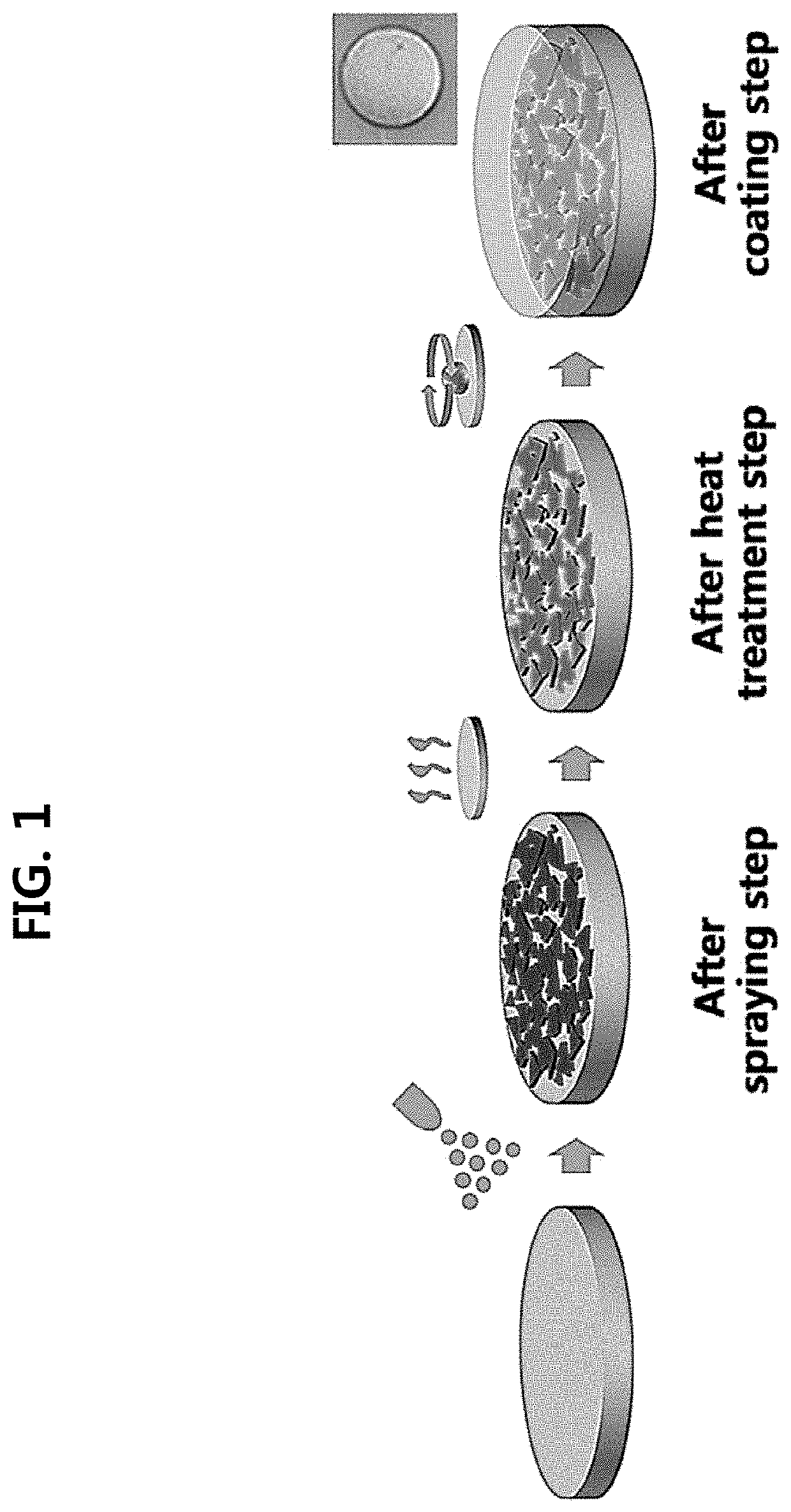
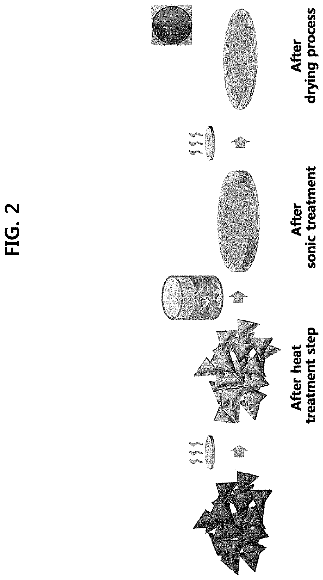
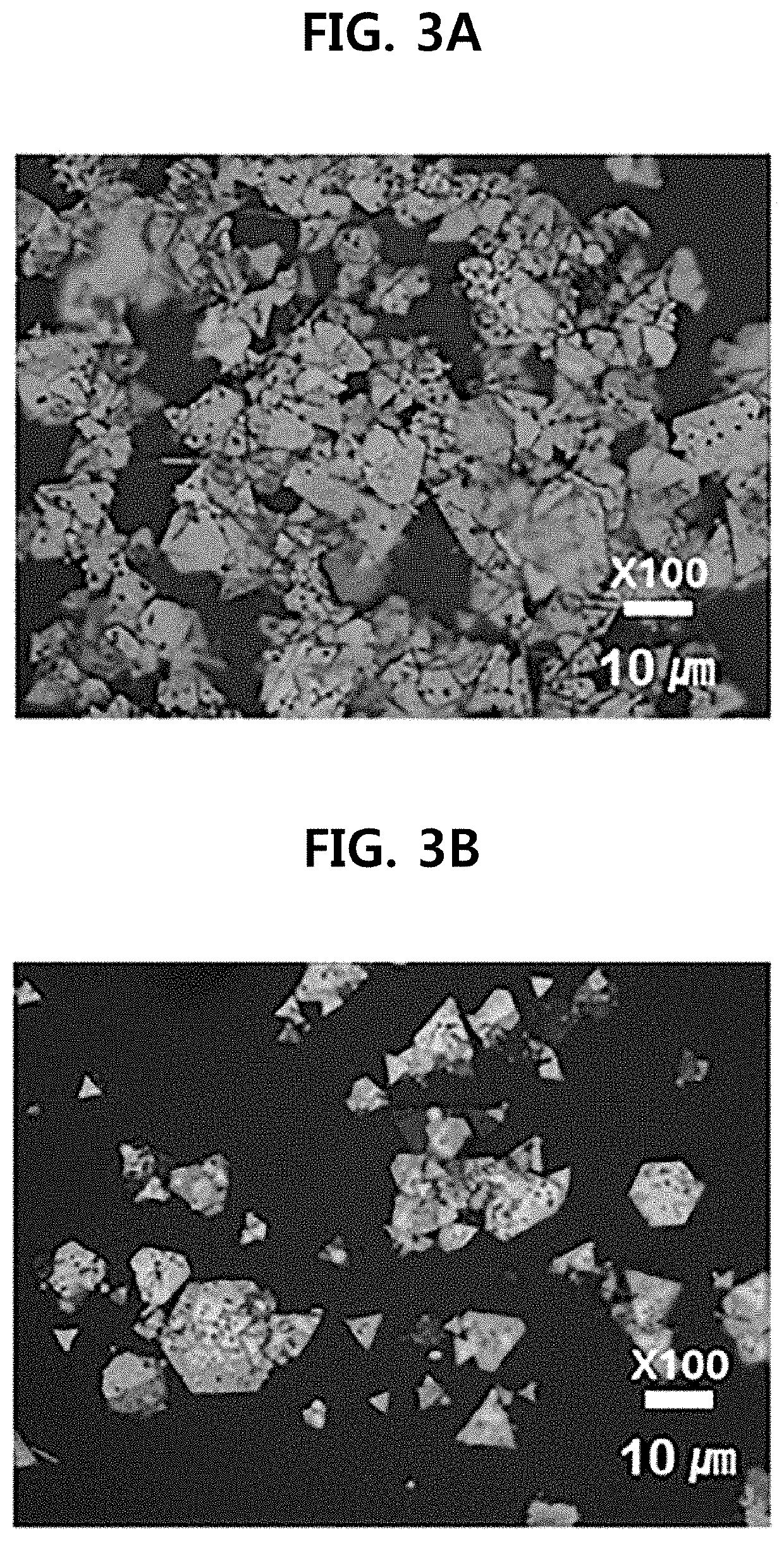
[0158]A mixed solution of 60 ml of chloroform in which 0.2 g of copper nanoplate (FIG. 3A to FIG. 4) was dispersed was prepared, and a polyimide film having a thickness of 100 μm was cut into a size of 2 cm×2 cm. Thereafter, the polyimide film was placed on a hot plate at 60° C., and a mixed solution in which the copper nanoplate was dispersed was spray-coated on the upper surface of the polyimide film 10 times in total by spraying 1 ml for each time. And then it was subjected to a heat treatment for one hour in a furnace at 250° C. in which argon / hydrogen flowed at a ratio of 95:5 to manufacture an electromagnetic wave shielding layer. Thereafter, the surface protective layer (SU-8) was coated on the electromagnetic wave shielding layer under the condition of 500 rpm / 5 s-2000 rpm / 30 s, followed by heat treatment for 3 minutes and 30 seconds on a 95° C. hot plate, UV treatment for 3 minutes, and heat treatment for 4 minutes and 30 seconds on a 95° C. hot plate to manufacture an elec...

example 2-5

[0159]The same process as in Example 1 was carried out except that the copper nanoplate spray coating process was carried out 2 times, 4 times, 6 times, and 8 times with 1 ml per each time to manufacture the electromagnetic wave shielding film according to Examples 2 to 5 (Example 2: 2 times, Example 3: 4 times, Example 4: 6 times, Example 5: 8 times).

example 6

[0160]The same process as in Example 3 was carried out except that a heat treatment was performed for one hour in a 200° C. furnace in which argon and hydrogen flowed at a ratio of 95:5 between the copper nanoplate spray coating and the SU-8 coating process to manufacture the electromagnetic wave shielding film.


PUM

PropertyMeasurementUnit
diameteraaaaaaaaaa
temperatureaaaaaaaaaa

Abstract

Provided is a method for manufacturing an electromagnetic interference shielding film comprising an electromagnetic interference shielding layer, the method comprising the steps of: preparing a metal nanoplate solution comprising a solvent in which metal nanoplates are dispersed; and coating the metal nanoplate solution on a substrate.

Description

CROSS-REFERENCE TO RELATED APPLICATION[0001]This application is a continuation of U.S. application Ser. No. 16 / 630,104, filed on Jan. 10, 2020, which was a National Stage application of PCT / KR2018 / 016584, filed on Dec. 24, 2018, and claims priority to Korean Patent Application No. 10-2018-0001674, filed on Jan. 5, 2018 and Korean Patent Application No. 10-2018-0158285, filed on Dec. 10, 2018, and all the benefits accruing therefrom under 35 U.S.C. § 119, the contents of which in its entirety are herein incorporated by reference.TECHNICAL FIELD[0002]Disclosed relates to a method of manufacturing a new electromagnetic wave shielding film.BACKGROUND ART[0003]Due to the miniaturization of electronic products and the development of information and communication devices, the pollution caused by electromagnetic waves in everyday life is increasing. These electromagnetic waves cause a malfunction or system errors of peripheral devices, and can cause diseases in the human body, which are dir...

Claims


Application Information

Patent Timeline
Patent Type & Authority Applications(United States)
IPC IPC(8): H05K9/00H01B13/30H01B13/22
CPCH05K9/0083H01B13/228H01B13/30B05D1/02B05D3/02B05D7/24H05K9/0092B05D3/0254B05D3/06
Inventor CHOI, HO-KOANGMOON, BYUNG JOONLEE, DONG SUBAE, SUKANGLEE, SEOUNG-KILEE, SANG HYUNKIM, TAE-WOOK
Owner KOREA INST OF SCI & TECH
Learn More