
Method of growing crystalline layers on amorphous substrates using two-dimensional and atomic layer seeds

a technology of amorphous substrates and crystalline layers, applied in the direction of crystal growth process, polycrystalline material growth, chemically reactive gases, etc., can solve the problems of significant limitations in the synthesis of high-quality single-crystalline group iii-v films, lack of native substrates, and significant limitations in the synthesis of nitride materials. achieve the effect of enhancing chemical vapor deposition

Active Publication Date: 2021-07-15
PENN STATE RES FOUND
View PDF0 Cites 4 Cited by
  • Summary
  • Abstract
  • Description
  • Claims
  • Application Information

AI Technical Summary

Benefits of technology

The patent describes a method to grow high-quality single-crystal or polycrystalline layers of Group III-V material on silicon dioxide or silicon substrates. This is achieved by using a thin layer of a Group III chalcogenide that can be annealed in NH3 to form a nanocrystalline layer, which serves as a seed layer for subsequent growth of the crystalline layer. This method allows for the transformation of the seed layer through epitaxial growth, which can be carried out using various techniques such as HVPE, MOCVD, PECVD, MBE, liquid phase exfoliation, and remote epitaxy. The resulting thin film can be used in various applications such as opto-electronics and electronics.

Problems solved by technology

However, there are significant limitations on the synthesis of high-quality single-crystalline Group III-V films.
First, there are significant limitations in nitride material synthesis.
A lack of native substrates and difficulty in further growing nitrides on native substrates stems largely from difficulties inherent to nitride synthesis—primarily the high nitrogen overpressure required to avoid film decomposition and to produce high-quality material as well as the low solubility of nitrogen in the respective metal.
Relatedly, there remains difficulty in growing the films on native substrates due to lattice mismatch.
Additionally, there is a significant problem stemming from the uncontrolled formation of amorphous SiNx, on the silicon surface due to lattice mismatch.
The layer of SiN, which is at most a few monolayers thick, forms spontaneously and is therefore difficult to control.
This layer typically is not uniform, and the surface coverage it provides is typically in the form of islands.
Even in a very clean system, i.e. with a low nitrogen background, formation of the Si—N bonds cannot be prevented.
There have been attempts to solve this problem, but none have been satisfactory.
For example the use of low temperature nucleation has been utilized; however, this method tends to result in uncontrolled domain structure and poor layer quality.
However, reliable and cost-effective methods have not yet been developed to utilize GIIIC materials in forming ultra-thin GaN layers.

Method used


Image

  • Method of growing crystalline layers on amorphous substrates using two-dimensional and atomic layer seeds
  • Method of growing crystalline layers on amorphous substrates using two-dimensional and atomic layer seeds
  • Method of growing crystalline layers on amorphous substrates using two-dimensional and atomic layer seeds

Examples


example 1

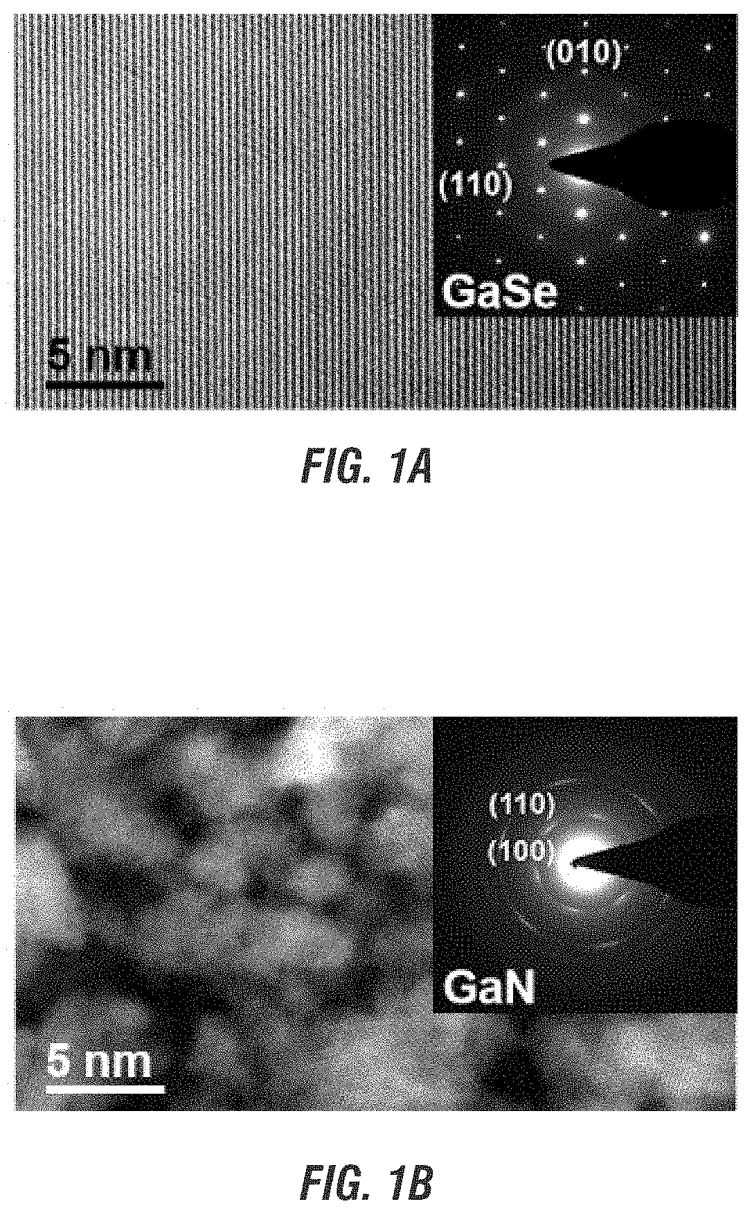
[0127]Single-crystal, mono- to few-layer GaSe layers were synthesized via powder vaporization of 7-12 mg bulk GaSe crystals placed beneath face-down 1×1 cm substrates of 300 nm SiO2 / Si or epitaxial graphene on SiC. GaSe crystal powders were vaporized beneath the substrates at temperatures from 700-850° C. for 30 minutes, under a constant flow of 200 sccm Ar and a pressure of 300 Torr. A ramp rate of 20° C. per minute was used to bring the furnace to growth temperature and the rate of rise of pressure in the tube furnace was ensured to be less than or equal to 5 mTorr per minute before each growth process. The furnace was cooled naturally to room temperature prior to sample removal.

[0128]The GaSe layers were then placed in a tube furnace and heated to 600° C. at 600 Torr, under constant flow of Ar at 100 sccm. A furnace ramp rate of 200° C. per minute was maintained and 100 sccm of NH3 was introduced once the furnace reached nitridation temperature. The furnace was cooled naturally t...

example 2

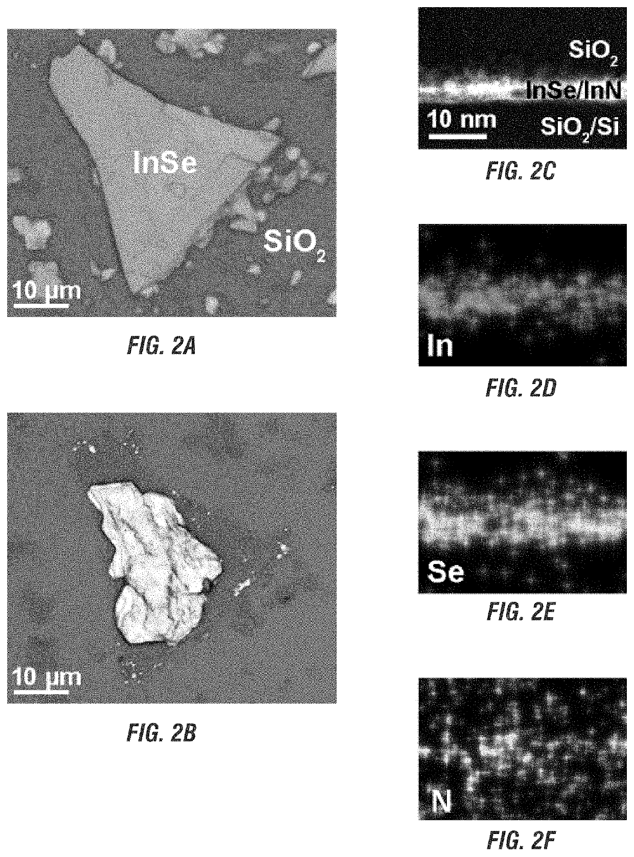
[0129]Exfoliated InSe layers were subjected to ammonolysis at temperatures above 500° C., leading to an etching effect of InSe layers rather than the transformation to InN, even at process times longer than 90 minutes, as shown in FIG. 2, indicating differences in atomic-level interactions between NH3 and different Group-III chalcogenides.

example 3

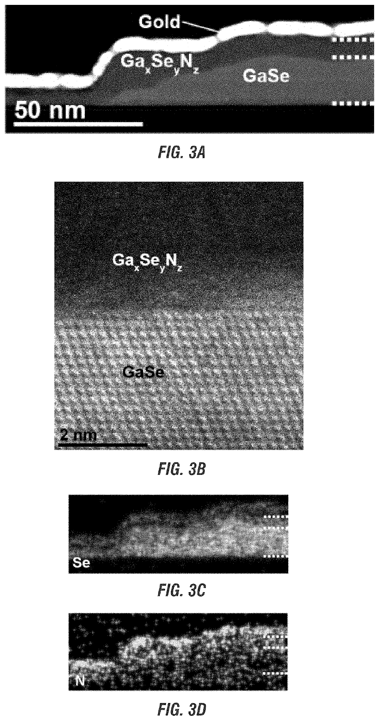
[0130]Multilayer GaSe exposed to NH3 for 30 minutes, not long enough for complete nitridation, exhibits a bilayer-type structure where the top layers are GaxSeyNz and the bottom layers remain single-crystal GaSe, as indicated in FIG. 3. Images (g) and (h) in FIG. 3 show Se deficiency in the outer, amorphous region along with a small nitrogen signal. This indicates the transformation involves the structural decomposition of GaSe followed by reaction with nitrogen. The presence of this amorphous, ternary outer layer in partially transformed bulk GaSe suggests that rather than the occurrence of a simple Se and N exchange, transformation to GaN requires significant structural changes.

[0131]Moreover, GaSe layers fabricated by exfoliation show nanocrystalline material following ammonolysis, as shown in FIG. 4, further indicating a chemical reaction and structural modification has taken place.


PUM

PropertyMeasurementUnit
thicknessaaaaaaaaaa
thicknessaaaaaaaaaa
thickaaaaaaaaaa

Abstract

This disclosure relates to methods of growing crystalline layers on amorphous substrates by way of an ultra-thin seed layer, methods for preparing the seed layer, and compositions comprising both. In an aspect of the invention, the crystalline layers can be thin films. In a preferred embodiment, these thin films can be free-standing.

Description

CROSS-REFERENCE TO RELATED APPLICATION[0001]This application is a Continuation of PCT / US19 / 53450 filed on Sep. 27, 2019, which claims priority under 35 U.S.C. § 119 to U.S. Provisional Application Ser. No. 62 / 738,846 filed on Sep. 28, 2019, each of which is hereby expressly incorporated by reference in its entirety, including, without limitation, the specification, claims, and abstract, as well as any figures, tables, or drawings thereof.GRANT REFERENCE[0002]This invention was made with government support under Grant No. DMR1539916 awarded by the National Science Foundation and under Grant No. W911NF-15-1-0488 awarded by the U.S. Army / ARO. The Government has certain rights in the invention.FIELD OF THE INVENTION[0003]The invention relates to a method of growing crystalline layers on amorphous substrates by way of an ultra-thin seed layer, methods for preparing the seed layer, and compositions of both.BACKGROUND OF THE INVENTION[0004]It has been well recognized that there are many be...

Claims


Application Information

Patent Timeline
Patent Type & Authority Applications(United States)
IPC IPC(8): H01L21/02
CPCH01L21/02568H01L21/02631C30B29/46C30B23/00C30B29/406C30B25/00H01L33/007H01L33/12H01L21/0254H01L31/03044H01L21/02381H01L21/02488H01L21/02485H01L21/02614H01L21/0262Y02E10/544C30B1/02C30B1/023
Inventor ROBINSON, JOSHUA A.BRIGGS, NATALIE
Owner PENN STATE RES FOUND
Learn More