
Photomask blank, and method of manufacturing photomask

Active Publication Date: 2020-06-18
SHIN ETSU CHEM CO LTD
View PDF0 Cites 0 Cited by
  • Summary
  • Abstract
  • Description
  • Claims
  • Application Information

AI Technical Summary

Benefits of technology

The invention provides a photomask blank with a chromium-containing film that can be easily shaped using dry etching with oxygen and chlorine. This results in a high-accuracy fine photomask pattern.

Problems solved by technology

In such a case, the pattern width varies in the pattern thickness direction, readily resulting in shape failure.
For patterning by using a pattern of the chromium-containing film as an etching mask, an underlying film, for example, a film composed of a material containing silicon and free of a transition metal, a film composed of a material containing a transition metal and silicon, or a transparent substrate is patterned, the pattering also has a problem such that dimensional deviation between a designed dimension and a dimension of the etched film or etched substrate becomes large, resulting in deterioration of pattern transferring performance.

Method used


Image

  • Photomask blank, and method of manufacturing photomask
  • Photomask blank, and method of manufacturing photomask
  • Photomask blank, and method of manufacturing photomask

Examples


example 1

[0087]First, a halftone phase shift film of SiN film (Si:N=47:53 (atomic ratio)) that has a phase shift of 177° and a transmittance of 19% (an optical density OD of 0.72), at a wavelength of 193 nm of ArF excimer laser, and a thickness of 60 nm was formed on a 6025 quartz substrate by sputtering in a DC sputtering apparatus. In this sputtering, a silicon target was used as a target, and argon gas and nitrogen gas were used as a sputtering gas. A discharge power was set to 2,000 W, and flow rates of argon gas and nitrogen gas were set to 15 sccm and 50 sccm, respectively.

[0088]Next, a chromium-containing film was formed on the halftone phase shift film by sputtering in a DC sputtering apparatus. In this sputtering, a chromium metal target was used as a target, and argon gas and carbon dioxide gas were used as a sputtering gas. A discharge power was set to 1,000 W and maintained in constant, a flow rate of argon gas was set to 10 sccm, and maintained in constant, and a flow rate of ca...

example 2

[0096]First, a halftone phase shift film of SiN film (Si:N=47:53 (atomic ratio)) that has a phase shift of 177° and a transmittance of 19% (an optical density OD of 0.72), at a wavelength of 193 nm of ArF excimer laser, and a thickness of 60 nm was formed on a 6025 quartz substrate by sputtering in a DC sputtering apparatus. In this sputtering, a silicon target was used as a target, and argon gas and nitrogen gas were used as a sputtering gas. A discharge power was set to 2,000 W, and flow rates of argon gas and nitrogen gas were set to 15 sccm and 50 sccm, respectively.

[0097]Next, a chromium-containing film was formed on the halftone phase shift film by sputtering in a DC sputtering apparatus. In this sputtering, a chromium metal target was used as a target, and argon gas and carbon dioxide gas were used as a sputtering gas. A discharge power was set to 1,000 W and maintained in constant, a flow rate of argon gas was set to 10 sccm, and maintained in constant, and a flow rate of ca...

example 3

[0105]First, a halftone phase shift film of SiN film (Si:N=47:53 (atomic ratio)) that has a phase shift of 177° and a transmittance of 19% (an optical density OD of 0.72), at a wavelength of 193 nm of ArF excimer laser, and a thickness of 60 nm was formed on a 6025 quartz substrate by sputtering in a DC sputtering apparatus. In this sputtering, a silicon target was used as a target, and argon gas and nitrogen gas were used as a sputtering gas. A discharge power was set to 2,000 W, and flow rates of argon gas and nitrogen gas were set to15 sccm and 50 sccm, respectively.

[0106]Next, a chromium-containing film was formed on the halftone phase shift film by sputtering in a DC sputtering apparatus. In this sputtering, a chromium metal target was used as a target, and argon gas, nitrogen gas and carbon dioxide gas were used as a sputtering gas. A discharge power was set to 1,000 W and maintained in constant, a flow rate of argon gas was set to 10 sccm, and maintained in constant, flow rat...


PUM


Abstract

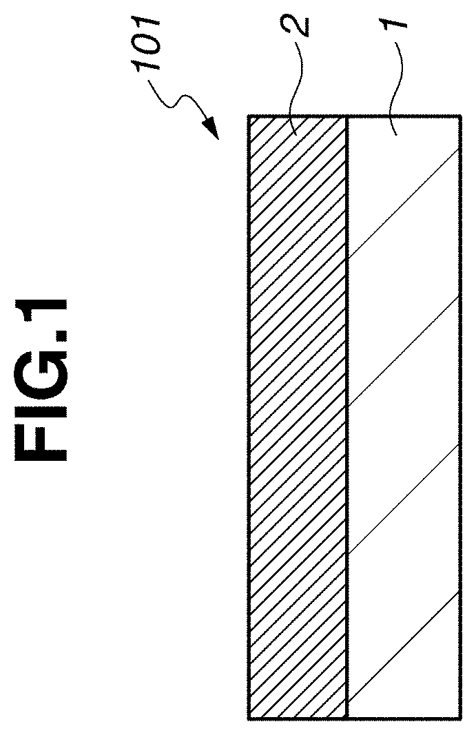
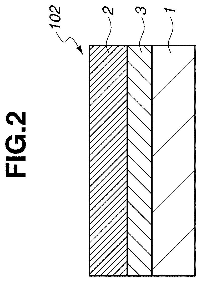
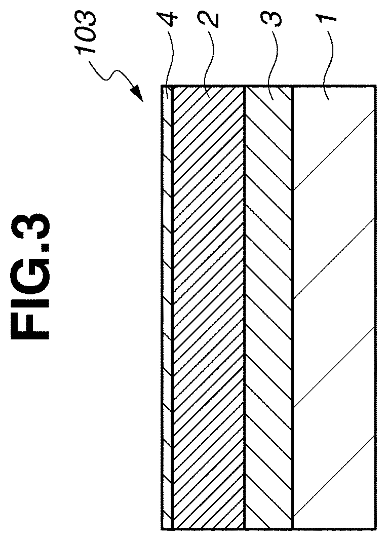
A photomask blank for a material of a photomask used in pattern transfer by exposure light having a wavelength of up to 250 nm, including a transparent substrate, a chromium-containing film directly formed on the substrate or formed with an optical film intervened between the transparent substrate and the chromium-containing film. The chromium-containing film includes a region (A) composed of a chromium compound containing chromium, oxygen and carbon, wherein each of contents of the elements contained in the chromium compound is continuously varied in the thickness direction of the region (A), and toward the substrate, the content of chromium increases, and the content of carbon decreases.

Description

CROSS-REFERENCE TO RELATED APPLICATION[0001]This non-provisional application claims priority under 35 U.S.C. § 119(a) on Patent Application No. 2018-232298 filed in Japan on Dec. 12, 2018, the entire contents of which are hereby incorporated by reference.TECHNICAL FIELD[0002]The present invention relates to a photomask blank which is a material in manufacturing a photomask for use in pattern transfer by exposure light, and a method of manufacturing a photomask using the same.BACKGROUND ART[0003]High integration of large scale integrated circuits is progressing for high-speed operation and low power consumption of semiconductor electronic devices. In connection with the miniaturization of circuit patterns, advanced semiconductor microfabrication technology has been become an extremely important elemental technology. For example, a finer technique for a wiring pattern constituting a circuit and a miniaturization technique for a contact hole pattern for wiring between layers constituti...

Claims


Application Information

Patent Timeline
IPC IPC(8): G03F1/50G03F1/48
CPCG03F1/48G03F1/50G03F1/26H01L21/027
Inventor INAZUKI, YUKIOSASAMOTO, KOUHEIMATSUHASHI, NAOKI
Owner SHIN ETSU CHEM CO LTD
Learn More