Hard-mask forming composition and method for manufacturing electronic component
- Summary
- Abstract
- Description
- Claims
- Application Information
AI Technical Summary
Benefits of technology
Problems solved by technology
Method used
Image
Examples
first embodiment
[0133]The method for manufacturing an electronic component according to the second aspect of the present invention includes steps of:
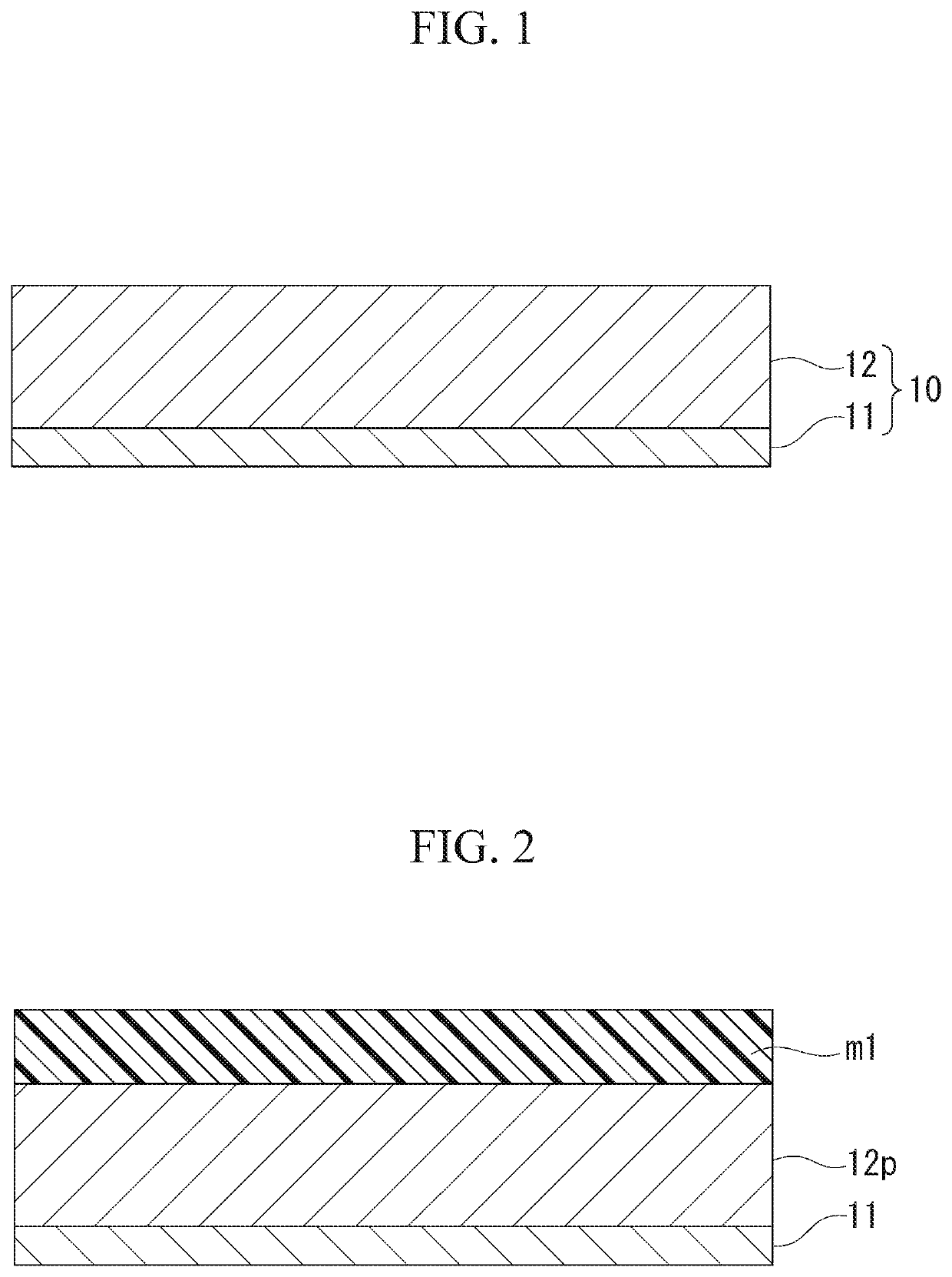
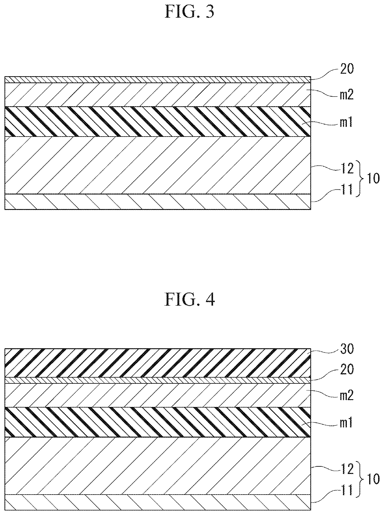
[0134]forming a hard mask layer (m1) on a support using the hard-mask forming composition according to the first aspect (hereinafter referred to as “step (i)”);
[0135]forming a hard mask layer (m2) made of an inorganic material on the hard mask layer (m1) (hereinafter referred to as “step (ii)”);
[0136]forming a resist film on the hard mask layer (m2) (hereinafter referred to as “step (iii)”);
[0137]forming a resist pattern on the hard mask layer (m2) by exposing and developing the resist film (hereinafter referred to as “step (iv)”);
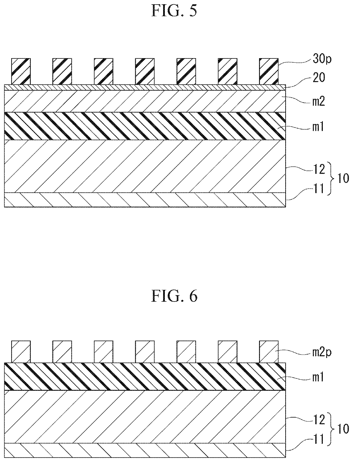
[0138]etching the hard mask layer (m2) with the resist pattern as a mask to form an inorganic pattern (hereinafter referred to as “step (v)”);
[0139]etching the hard mask layer (m1) with the inorganic pattern as a mask to form a resin pattern (hereinafter referred to as “step (vi)”); and
[0140]processing the support with the re...
second embodiment
[0194]The method for manufacturing an electronic component according to the third aspect includes steps of:
[0195]forming the hard mask layer (m1) on the support using the hard-mask forming composition according to the first aspect (hereinafter referred to as “step (i)”);
[0196]forming the inorganic pattern made of the inorganic material on the hard mask layer (m1) (hereinafter referred to as “step (v)”);
[0197]etching the hard mask layer (m1) with the inorganic pattern as a mask to form the resin pattern (hereinafter referred to as “step (vi)”); and
[0198]processing the support with the resin pattern as a mask (hereinafter referred to as “step (vii)”).
[0199]The method for manufacturing an electronic component according to the third aspect is the same as the method for manufacturing an electronic component according to the second aspect, except that the inorganic pattern made of the inorganic material is formed directly on the hard mask layer (m1) without forming the resist film.
[0200]A...
examples
[0207]Hereinafter, the present invention will be described in more detail referring to examples. However, the present invention is not limited to these examples.
Preparation Example of First Resin
[0208]10.00 g (34.09 mmol) of 9-naphthylcarbazole, 36.17 g (340.9 mmol) of benzaldehyde, and 66.96 g (306.8 mmol) of 1-pyrenol were dissolved in 75.42 g of propylene glycol monomethyl ether acetate (PGMEA). 87.53 g of 10% PGMEA solution of para-toluenesulfonic acid was added to the resultant mixture. Polymerization was carried out while maintaining the reaction temperature at about 120° C.
[0209]After reacting for about 10 hours, an excess amount of methanol / water (9:1) co-solvent was added to the reaction product, and the resultant solid was dissolved in an appropriate amount of PGMEA. The dissolved solid was added dropwise to an excess amount of ethanol / water (9:1) co-solvent, and the precipitate was collected. The precipitate was dried in a vacuum oven at about 65° C. for about 20 hours. A...
PUM
| Property | Measurement | Unit |
|---|---|---|
| Percent by mass | aaaaa | aaaaa |
| Percent by mass | aaaaa | aaaaa |
| Shrinkage | aaaaa | aaaaa |
Abstract
Description
Claims
Application Information
 - R&D
- Intellectual Property
- Life Sciences
- Materials
- Tech Scout
- Unparalleled Data Quality
- Higher Quality Content
- 60% Fewer Hallucinations
Browse by: Latest US Patents, China's latest patents, Technical Efficacy Thesaurus, Application Domain, Technology Topic, Popular Technical Reports.
© 2025 PatSnap. All rights reserved.Legal|Privacy policy|Modern Slavery Act Transparency Statement|Sitemap|About US| Contact US: help@patsnap.com


