
Photosensitive and via-forming circuit board

a technology of printed circuit boards and viaforming, which is applied in the field of circuit boards, can solve the problems of poor heat resistance and flexibility of printed circuit boards, and cannot meet the needs of the industry, and achieve the effect of enhancing heat resistance and flexibility of circuit boards

Active Publication Date: 2018-09-13
MICROCOSM TECH
View PDF5 Cites 2 Cited by
  • Summary
  • Abstract
  • Description
  • Claims
  • Application Information

AI Technical Summary

Benefits of technology

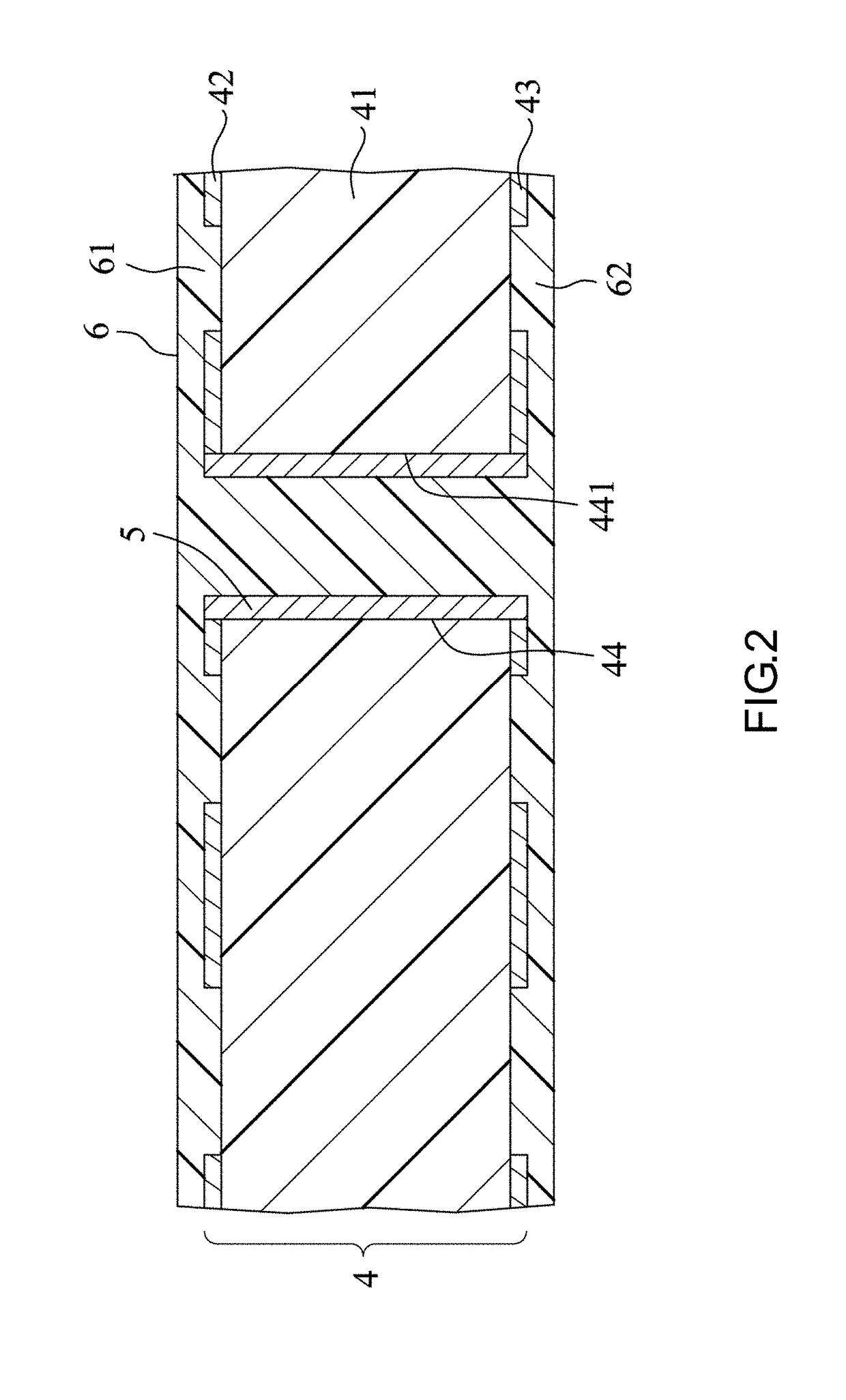
The present invention provides a photosensitive and via-forming circuit board that has improved flexibility and heat resistance. The circuit board has a photosensitive opening formed after a lithography process. An insulating layer, such as an epoxy resin layer or a polyimide resin layer, is used to form the circuit board, with the insulating layer being flexible. A second cover layer is formed on the second conductive wiring layer of the laminate unit to improve insulation. The cover layer unit not only protects the conductive layers but also acts as a plug piece to prevent air from entering the through hole. The invention also uses an epoxy group-containing compound to improve the heat resistance and acid resistance of the circuit board. Overall, the invention provides a flexible and heat-resistant circuit board with improved insulation properties.

Problems solved by technology

However, the main materials of the photosensitive solder resist 2 and the solder resist layers 3 described in the patent application were generally photocurable epoxy resins, such that the heat resistance and flexibility of the printed circuit board were poor and couldn't meet the industry's needs.

Method used


Image

  • Photosensitive and via-forming circuit board
  • Photosensitive and via-forming circuit board
  • Photosensitive and via-forming circuit board

Examples


synthesis example 1

[0043]16.95 g (0.111 mol) of 3,5-diaminobenzoic acid, 13.07 g (0.032 mol) of 2,2-bis[4-(4-aminophenoxy)phenyl]propane, 75.60 g (0.080 mol) of bisaminopropyltetramethyldisiloxane, and 126.72 g of N-methyl-2-pyrrolidone were mixed to form a homogeneous mixture. 46.61 g (0.188 mol) of bicyclo[2,2,2]oct-7-ene-2,3,5,6-tetracarboxylic dianhydride was added to the homogeneous mixture, which was then mixed for 2 hours. Afterwards, 14.85 g (0.033 mol) of 4,4′-(hexafluoroisopropylidene)diphthalic anhydride was added and mixed for 4 hours at room temperature. After that, 65 g of xylene was added and then heated to the temperature for the polymerization reaction and mixed for 3 to 6 hours. After the temperature was down to 80° C., 7.92 g (0.056 mol) of glycidyl (meth)acrylate was added and then mixed between 80° C. to 120° C. for 12 hours. Next, the temperature was down to 25° C. and 301.72 g of the constituent containing the photosensitive polyimide was obtained. The solid content of the const...

synthesis example 2

[0044]16.45 g (0.108 mol) of 3,5-diaminobenzoic acid, 6.77 g (0.032 mol) of 1,3-bis(4′-aminophenoxy)benzene, 80.70 g (0.085 mol) of bisaminopropyltetramethyldisiloxane, and 168.14 g of N-methyl-2-pyrrolidone were mixed to form a homogeneous mixture. 46.93 g (0.178 mol) of 5-(2,5-dioxotetrahydro-3-furanyl)-3-methyl-3-cyclohexene-1,2-dicarboxylic anhydride was added to the homogeneous mixture, which was then mixed for 2 hours. Afterwards, 16.46 g (0.037 mol) of 4,4′-(hexafluoroisopropylidene)diphthalic anhydride was added and mixed for 4 hours at room temperature. After that, 65 g of xylene was added and then heated to the temperature for the polymerization reaction and mixed for 3 to 6 hours. After the temperature was down to 80° C., 7.68 g (0.054 mol) of glycidyl (meth)acrylate was added and then mixed between 80° C. to 120° C. for 12 hours. Next, the temperature was down to 25° C. and 343.13 g of the constituent containing the photosensitive polyimide was obtained. The solid conten...

synthesis example 3

[0045]18.62 g (0.122 mol) of 3,5-diaminobenzoic acid, 17.94 g (0.044 mol) of 2,2-bis[4-(4-aminophenoxy)phenyl]propane, 74.73 g (0.079 mol) of bisaminopropyltetramethyldisiloxane, and 231.98 g of N-methyl-2-pyrrolidone were mixed to form a homogeneous mixture. 41.82 g (0.213 mol) of cyclobutane-1,2,3,4-tetracarboxylic dianhydride was added to the homogeneous mixture, which was then mixed for 2 hours. Afterwards, 13.20 g (0.030 mol) of 4,4′-(hexafluoroisopropylidene)diphthalic anhydride was added and mixed for 4 hours at room temperature. After that, 65 g of xylene was added and then heated to the temperature for the polymerization reaction and mixed for 3 to 6 hours. After the temperature was down to 80° C., 8.70 g (0.061 mol) of glycidyl (meth)acrylate was added and then mixed between 80° C. to 120° C. for 12 hours. Next, the temperature was down to 25° C. and 406.99 g of the constituent containing the photosensitive polyimide was obtained. The solid content of the constituent conta...


PUM

PropertyMeasurementUnit
Diameteraaaaaaaaaa
Diameteraaaaaaaaaa
Flexibilityaaaaaaaaaa

Abstract

A photosensitive and via-forming circuit board comprising a laminate unit, a conductor unit, and a cover layer unit is provided. The laminate unit includes an insulating layer, a first conductive wiring layer and a second conductive wiring layer formed at two opposite sides of the insulating layer, respectively, and at least one through-hole surface defining a through hole extending from the upper surface of the first conductive wiring layer through the insulating layer to the lower surface of the second conductive wiring layer. The conductor unit is formed on the at least one through-hole surface. The cover layer unit is formed from a photosensitive composition comprising an epoxy group-containing compound and a photosensitive polyimide capable of reacting with the epoxy group of the epoxy group-containing compound, and includes a first cover layer formed on the first conductive wiring layer and extending into and filling the through hole.

Description

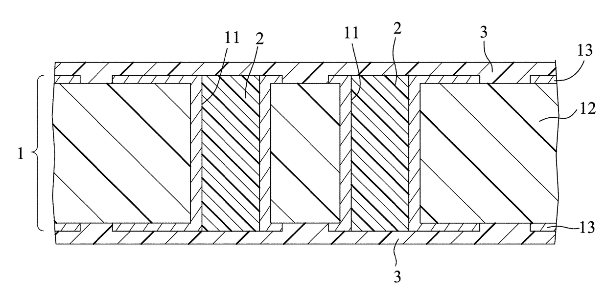
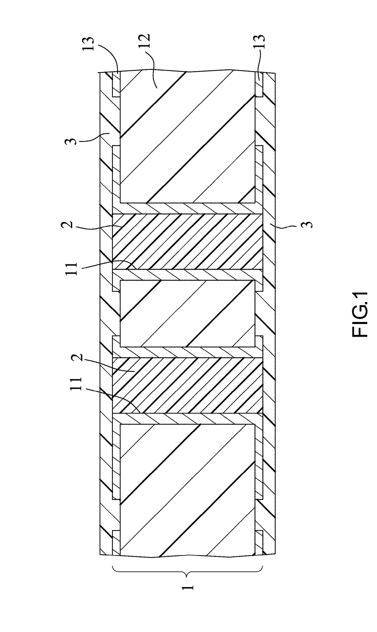
BACKGROUND OF THE INVENTIONField of the Invention[0001]The present invention relates to a circuit board and, more particularly, to a photosensitive and via-forming circuit board.Description of the Prior Art[0002]Referring to FIG. 1, a printed circuit board was disclosed in the Taiwan patent publication No. 201316858, which comprised a laminate 1 defining a plurality of electrical through holes 11 that are spaced, the photosensitive solder resist 2 filling the electrical through holes 11, and two solder resist layers 3 formed at two opposite sides of the laminate 1. The laminate 1 included an insulating substrate 12 and two wiring conductor layers 13 formed at two opposite sides of the insulating substrate 12. However, the main materials of the photosensitive solder resist 2 and the solder resist layers 3 described in the patent application were generally photocurable epoxy resins, such that the heat resistance and flexibility of the printed circuit board were poor and couldn't meet ...

Claims


Application Information

Patent Timeline
IPC IPC(8): H05K3/46H05K1/02H05K3/40H05K1/03H05K3/10C08G73/10C08G59/40C08G59/24C08G59/22G03F7/20G03F7/038G03F7/039G03F7/32G03F7/16
CPCH05K3/4644H05K2201/0154H05K3/4038H05K1/0353H05K3/10C08G73/105C08G73/1042C08G73/1039C08G73/106C08G73/1028C08G59/4042C08G59/245C08G59/22G03F7/2004G03F7/0387G03F7/039G03F7/322G03F7/16G03F7/168H05K1/028H05K1/0393H05K1/112H05K3/287H05K3/3452H05K2201/0959H05K2203/0582G03F7/038G03F7/0757C09D179/08C08G73/1075C08L63/00Y10T428/31681Y10T428/31721
Inventor HUANG, TANG-CHIEH
Owner MICROCOSM TECH
Learn More