
Systems, methods and apparatus for use with superconducting based computing systems

a computing system and superconducting technology, applied in shielding materials, magnetic bodies, instruments, etc., can solve the problems of compounding difficulties, difficult to maintain superconducting temperatures, and especially difficult with i/o systems

Active Publication Date: 2017-06-22
D WAVE SYSTEMS INC
View PDF0 Cites 19 Cited by
  • Summary
  • Abstract
  • Description
  • Claims
  • Application Information

AI Technical Summary

Benefits of technology

The patent describes a method and apparatus for reducing high frequency noise in a GHz range at non-galvanic connections between electronics at or above a temperature of 15°C and processors operating at or below 0°C. The apparatus includes a toroidal core and a first and second windings, which are electrically coupled to a noise insulating transformer that reduces high frequency noise. The apparatus also includes a high conductive shielding wall, a tubular filter, a metal power-epoxy mixture, and an absorptive layer. The method includes measuring resistance through a substrate on which a processor is mounted via a clamp with adjustable fasteners, adjusting the force applied by each fastener, measuring resistance after adjusting the force, and adjusting the torque on the fasteners to balance thermal current. The technical effects of the patent include reducing high frequency noise in electronic circuits and improving thermal management.

Problems solved by technology

Maintaining superconducting temperatures may be difficult since many materials that are capable of superconducting do not provide good thermally conductive paths.
Such may be particularly difficult with I / O systems since I / O systems typically interface with non-refrigerated environments.
Such difficulties are compounded where the structure is also to provide for the easy placement and removal of a superconducting processor.
For instance, environments of extreme heat can cause even the strongest and most solid materials to melt away or disperse as gas.
The pumps and compressors used are large, expensive, noisy, in need of periodic maintenance, and they inevitably add contaminants, such as air (i.e., nitrogen, oxygen, carbon dioxide, argon, etc.) to the helium.
These contaminants typically have higher freezing points than the helium and so may solidify in the helium fluid channels, creating blockages.
Such blockages may plug fine capillaries in the dilution refrigerator, causing problems with reliability.
The procedure of warming and subsequently cooling back down to operating temperatures can take several days.
Filters and cold traps can be used to reduce the frequency of plugging by removing contaminants from the helium, but existing filters and traps used in the art are of limited effectiveness.
Thus, plugging due to contaminants remains a serious technical challenge in cryogenic refrigeration technology affecting refrigerator performance, and there remains a need in the art for improved systems and methods for contaminant filtering and / or trapping in cryogenic refrigeration systems.
However, single-ended signaling can be highly susceptible to noise that is picked up (during transmission) by the signal wire and / or the ground path, as well as noise that results from fluctuations in the ground voltage level throughout the system.
Thus, any fluctuations in the signal and / or reference voltage that occur between sending and receiving the signal can result in a discrepancy between the signal that enters the signal wire and the signal that is received by the receiving circuit.
Thus, if the first wire and the second wire are maintained in close physical proximity throughout the signal transmission, any noise coupled to the data signal is likely also to couple to the reference signal and therefore any such noise may be cancelled out in the receiving circuit.
The main disadvantage of differential signaling is that it uses approximately twice as many wires as single-ended signaling.
However, in some applications this disadvantage is more than compensated by the improved signal-to-noise ratio of differential signaling.
The inner inductor will have significantly lower stray capacitance before it is shielded from the wall of the enclosure by the outer inductor, causing an increased ripple in pass-band filtering, thus decreasing the effectiveness of the filter.
Due to issues unique to superconducting circuits, not all semiconductor processes and techniques are necessarily transferable to superconductor chip manufacture.
Such changes and adjustments typically are not obvious and may require a great deal of experimentation.
Any impurities within superconducting chips may result in noise which can compromise or degrade the functionality of the individual devices, such as superconducting qubits, and of the superconducting chip as a whole.
Magnetic fields produced by external sources may cause unwanted interactions with devices in the integrated circuit.
The quantum properties of quantum devices are very sensitive to noise, and stray magnetic fields in superconducting quantum devices can negatively impact the quantum information processing properties of such circuits.
However, such approaches have only been used in superconducting integrated circuits for classical processing and sensor applications, which are relatively robust against in-circuit noise and operate at significantly higher temperatures as compared with superconducting quantum processing integrated circuits.
In superconducting quantum processing integrated circuits, it is desirable to substantially attenuate and control unwanted cross-talk between devices, otherwise quantum information processing at commercial scales may not be possible.

Method used


Image

  • Systems, methods and apparatus for use with superconducting based computing systems
  • Systems, methods and apparatus for use with superconducting based computing systems
  • Systems, methods and apparatus for use with superconducting based computing systems

Examples


Embodiment Construction

Non Dissipative Differential Filters

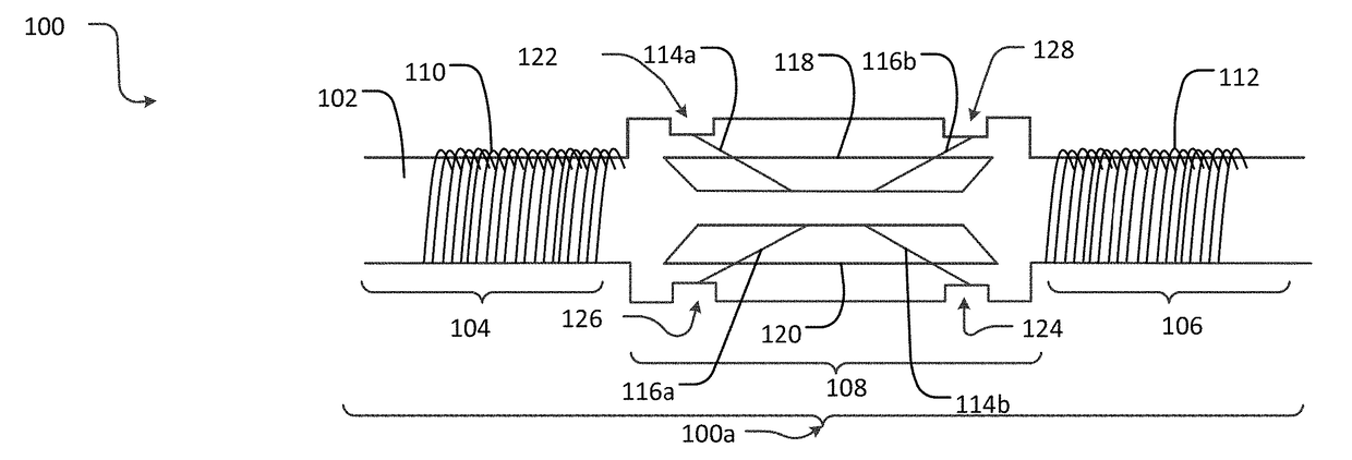
[0141]In the following description, some specific details are included to provide a thorough understanding of various disclosed embodiments. One skilled in the relevant art, however, will recognize that embodiments may be practiced without one or more of these specific details, or with other methods, components, materials, etc. In other instances, well-known structures associated with superconducting processors, such as superconducting devices, coupling devices, and control systems including microprocessors and drive circuitry have not been shown or described in detail to avoid unnecessarily obscuring descriptions of the embodiments of the systems, devices, and methods.

[0142]Unless the context requires otherwise, throughout the specification and claims which follow, the word “comprise” and variations thereof, such as, “comprises” and “comprising” are to be construed in an open, inclusive sense, that is as “including, but not limited to.”

[0143]Refe...


PUM


Abstract

An electrical filter includes a dielectric substrate with inner and outer coils about a first region and inner and outer coils about a second region, a portion of cladding removed from wires that form the coils and coupled to electrically conductive traces on the dielectric substrate via a solder joint in a switching region. An apparatus to thermally couple a superconductive device to a metal carrier with a through-hole includes a first clamp and a vacuum pump. A composite magnetic shield for use at superconductive temperatures includes an inner layer with magnetic permeability of at least 50,000; and an outer layer with magnetic saturation field greater than 1.2 T, separated from the inner layer by an intermediate layer of dielectric. An apparatus to dissipate heat from a superconducting processor includes a metal carrier with a recess, a post that extends upwards from a base of the recess and a layer of adhesive on top of the post. Various cryogenic refrigeration systems are described.

Description

BACKGROUNDField[0001]This disclosure generally relates to systems and articles for use with superconducting devices, and particularly relates to electrical filters, I / O systems, magnetic shielding and cryogenic systems for use with superconducting-based computing systems.Superconducting Qubits[0002]There are many different hardware and software approaches under consideration for use in quantum computers. One hardware approach employs integrated circuits formed of superconducting material, such as aluminum and / or niobium, to define superconducting qubits. Superconducting qubits can be separated into several categories depending on the physical property used to encode information. For example, superconducting qubits may be separated into charge, flux and phase devices. Charge devices store and manipulate information in the charge states of the device; flux devices store and manipulate information in a variable related to the magnetic flux through some part of the device; and phase dev...

Claims


Application Information

Patent Timeline
IPC IPC(8): G06N99/00H01L39/12H01L39/24H05K3/34H05K9/00F25B43/00H01L39/18H01F41/06H01F41/04H01F13/00F25B9/12H03H3/00H05K1/02
CPCG06N99/002H05K2203/085H01L39/12H01L39/2406H05K3/341H05K9/0075H05K1/0203H01L39/18H01F41/06H01F41/048H01F13/006F25B9/12F25B43/003H03H2001/005H03H3/00H05K1/0233H05K1/0245H05K1/16H05K2201/10287H03H7/425H01F41/076G06N10/00H10N60/80H10N60/20
Inventor TCACIUC, ALEXANDR M.DE BUEN, PEDRO A.SPEAR, PETER D.UCHAYKIN, SERGEY V.ENDERUD, COLIN C.NEUFELD, RICHARD D.HILTON, JEREMY P.PETROFF, J. CRAIGKAMDAR, AMAR B.PEREGRYM, GREGORY D.KAN, EDMOND HO YINSWENSON, LOREN J.STERLING, GEORGE E.G.CITVER, GREGORY
Owner D WAVE SYSTEMS INC
Learn More