Film capacitor
a film capacitor and capacitor technology, applied in the field of film capacitors, can solve the problems of inability to the inability to reliably ensure the desired capacitance, and the likelihood of remaining, so as to achieve the effect of reducing the air gap, ensuring the desired capacitance, and increasing the contactability
- Summary
- Abstract
- Description
- Claims
- Application Information
AI Technical Summary
Benefits of technology
Problems solved by technology
Method used
Image
Examples
first embodiment
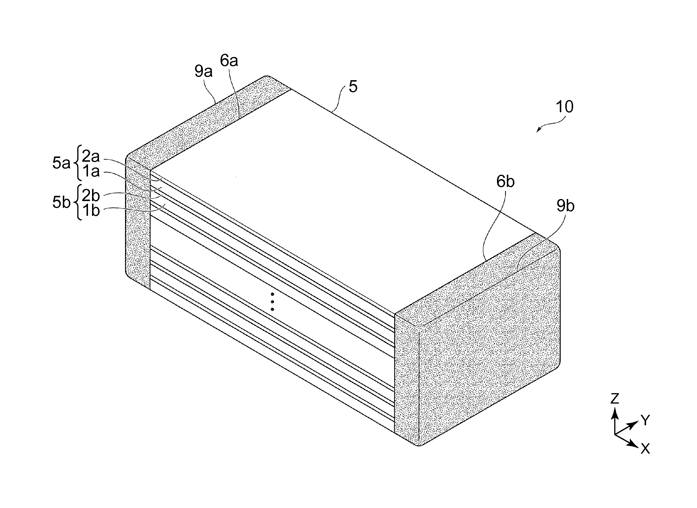
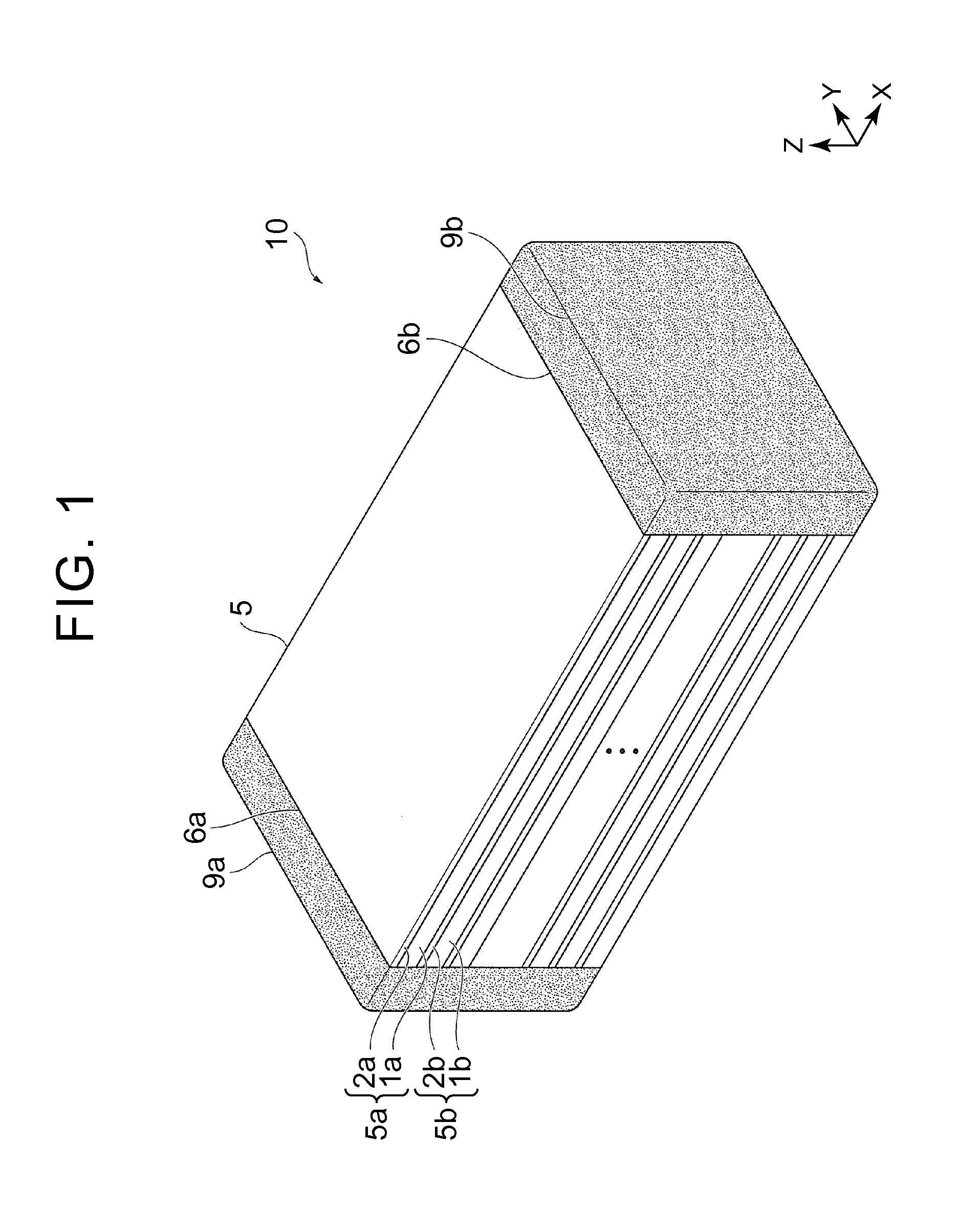
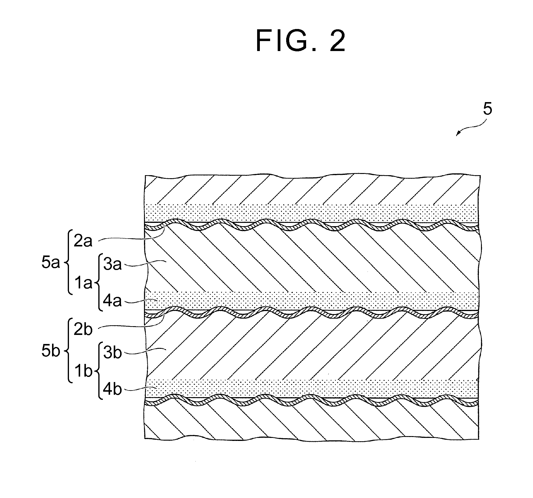
[0035]Thus, in the film capacitor 10 according to the invention, each of the dielectric films 1a and 1b includes the high dielectric layer 3a or 3b that has a relatively high content of the high dielectric filler, and the low dielectric layer 4a or 4b that has a relatively low content of the high dielectric filler or that does not contain the high dielectric filler. The low dielectric layer 4a or 4b, which is relatively flexible, is provided on the outermost surface of the high dielectric layer 3a or 3b, the outermost surface being located on the side opposite to the metal electrode 2a or 2b (in other words, the low dielectric layer 4a or 4b is provided on the opposite side of the high dielectric layer 3a or 3b from the metal electrode 2a or 2b). Thus, when the metalized films 5a and 5b that include the dielectric films 1a and 1b containing the high dielectric filler are stacked to produce the film capacitor 10, the low dielectric layer 4a or 4b that is provided in the reverse surfa...
second embodiment
[0037]In this second embodiment of the invention, each of dielectric films 1aA and 1bA constituting a stacked body 5A of the film capacitor 10A includes a high dielectric layer 3aA or 3bA that has a relatively high content (a relatively high content percentage) of a high dielectric filler (i.e., the high dielectric layer 3aA or 3bA that has high electric permittivity), and a low dielectric layer 4aA or 4bA that has a relatively low content (a relatively low content percentage) of the high dielectric filler or that does not contain the high dielectric filler (i.e., the low dielectric layer 4aA or 4bA that has low electric permittivity). The low dielectric layer 4aA or 4bA is provided between the high dielectric layer 3aA or 3bA and the metal electrode 2aA or 2bA (i.e., the low dielectric layer 4aA or 4bA is provided in the surface side of the dielectric film 1aA or 1bA). That is, each of the dielectric films 1aA and 1bA has a double-layer structure consisting of the high dielectric l...
third embodiment
[0040]In the invention, each of dielectric films 1aB and 1bB constituting a stacked body 5B of the film capacitor 10B includes a high dielectric layer 3aB or 3bB that has a relatively high content (a relatively high content percentage) of a high dielectric filler (i.e., the high dielectric layer 3aB or 3bB that has high electric permittivity), and two low dielectric layers 4aaB or 4baB and 4abB or 4bbB that have a relatively low content (a relatively low content percentage) of the high dielectric filler or that do not contain the high dielectric filler (i.e., the two low dielectric layers 4aaB or 4baB and 4abB or 4bbB that have low electric permittivity). One of the low dielectric layers 4aaB or 4baB is provided between the high dielectric layer 3aB or 3bB and the metal electrode 2aB or 2bB (i.e., one of the low dielectric layers 4aaB or 4baB is provided in the surface side of the dielectric film 1aB or 1bB). The other low dielectric layer 4abB or 4bbB is provided on the outermost s...
PUM
| Property | Measurement | Unit |
|---|---|---|
| thickness | aaaaa | aaaaa |
| dielectric | aaaaa | aaaaa |
| electrical characteristics | aaaaa | aaaaa |
Abstract
Description
Claims
Application Information
 - R&D
- Intellectual Property
- Life Sciences
- Materials
- Tech Scout
- Unparalleled Data Quality
- Higher Quality Content
- 60% Fewer Hallucinations
Browse by: Latest US Patents, China's latest patents, Technical Efficacy Thesaurus, Application Domain, Technology Topic, Popular Technical Reports.
© 2025 PatSnap. All rights reserved.Legal|Privacy policy|Modern Slavery Act Transparency Statement|Sitemap|About US| Contact US: help@patsnap.com


