Strip-shaped gate tunneling field effect transistor with double-diffusion and a preparation method thereof

a field effect transistor and double-diffusion technology, which is applied in the direction of semiconductor devices, diodes, electrical apparatuses, etc., can solve the problems of increasing device power consumption, power consumption concerns, and negative effects such as short channel effect of devices, and achieves steep energy band bending, large tunneling area, and increased process steps

Inactive Publication Date: 2015-02-19
PEKING UNIV
View PDF5 Cites 1 Cited by
  • Summary
  • Abstract
  • Description
  • Claims
  • Application Information

AI Technical Summary

Benefits of technology

[0021]Firstly, with the same active area, the device can achieve a larger tunneling area by using a strip-shaped gate extending into the source region, and then can obtain a turn-on current higher than that of the conventional TFET; and by implanting the double-diffusing impurities with the opposite doping type into the source region, the device can obtain a steeper energy band bending at the source tunnel junction, thereby the electric field when the band-to-band tunneling occurs in the device is larger, and the sub-threshold slope and the on-state current of the TFET device can be further improved.
[0022]Secondly, without increasing the process steps, only through simply designing of layout (i.e., the strip-shaped gate profile), the energy band of the channel on the gate lower surface is improved by PN junction depletion effect on both sides of the strip-shaped gate, so the device may obtain a steeper energy band and a narrower tunneling barrier width than the traditional TFET when the band-to-band tunneling occurs, equivalently achieving the effect of a steep doping concentration gradient at the tunneling junction, and thereby the sub-threshold characteristics of the conventional TFET are significantly improved;
[0023]Thirdly, the preparation process of the device is simple, and the preparation method is fully compatible with the conventional MOSFET process.
[0024]In short, the device structure modulates the source-side tunneling junction of the conventional TFET device by using the strip-shaped gate structure and the double-diffusion source, achieves the effects that there are the steeper energy band bending and the larger tunneling electric field at the source junction, and greatly improves the TFET device performance; and the preparation method thereof is simple. Compared with the conventional TFET, in the case of the same process conditions, the same process steps and the same size of the active region, the device can obtain a higher turn-on current and a steeper sub-threshold slope, and can maintain a lower leakage current. This device can be expected to be adopted in the field of the low power consumption, and has a higher practical value.

Problems solved by technology

Under the drive of Moore's Law, the feature size of the conventional MOSFET continues to shrink, now has to enter the nanometer scale, consequently, the negative effects such as short channel effect of a device and so on have become more serious.
The effects of drain induced barrier lowering, band-to-band tunneling and so on cause a off-state leakage current of a device to increase continually, at the same time, a sub-threshold slope of the conventional MOSFET can not decrease synchronously with the shrink of the device size due to of the limitation by the thermal potential, thereby the device power consumption increases.
Now the power consumption concern has become the most serious problem of limiting the device shrink by the same scale.
However, due to the limitation of source junction tunneling probability and tunneling area, TFET is faced with a problem of small on-state current, which is far less than the traditional MOSFET devices, and this greatly limits the applications of TFET device.
In addition, it is difficult to achieve TFET device with a steep sub-threshold slope in the experiment, because it is more difficult to achieve a steep doping concentration gradient at the source junction in the experiment so that the electric field at the tunneling junction is not sufficiently large when the device turns on, which may cause a sub-threshold slope of TFET to degrade relative to the theoretical value.
Therefore, it has become a further important issue in connection with TFET device how to achieve a steep doping concentration gradient at the source junction to obtain an ultra-low sub-threshold slope.

Method used


Image

  • Strip-shaped gate tunneling field effect transistor with double-diffusion and a preparation method thereof
  • Strip-shaped gate tunneling field effect transistor with double-diffusion and a preparation method thereof
  • Strip-shaped gate tunneling field effect transistor with double-diffusion and a preparation method thereof

Examples


Embodiment Construction

[0035]Hereinafter, the present invention will be further illustrated by the examples. It is noted that, the disclosed embodiments are intended to help further understand the present invention, but it will be appreciated to those skilled in the art that various substitutes and modifications may be made without departing from the spirit and scope defined by the present invention and the following claims. Accordingly, the present invention should not be limited to the contents disclosed by the embodiments, and the protected scope of the present invention should be defined by the claims.

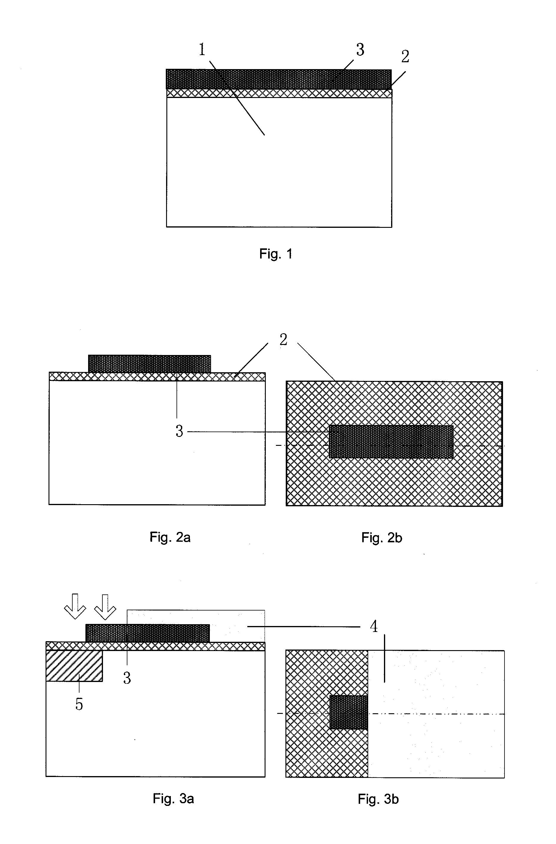
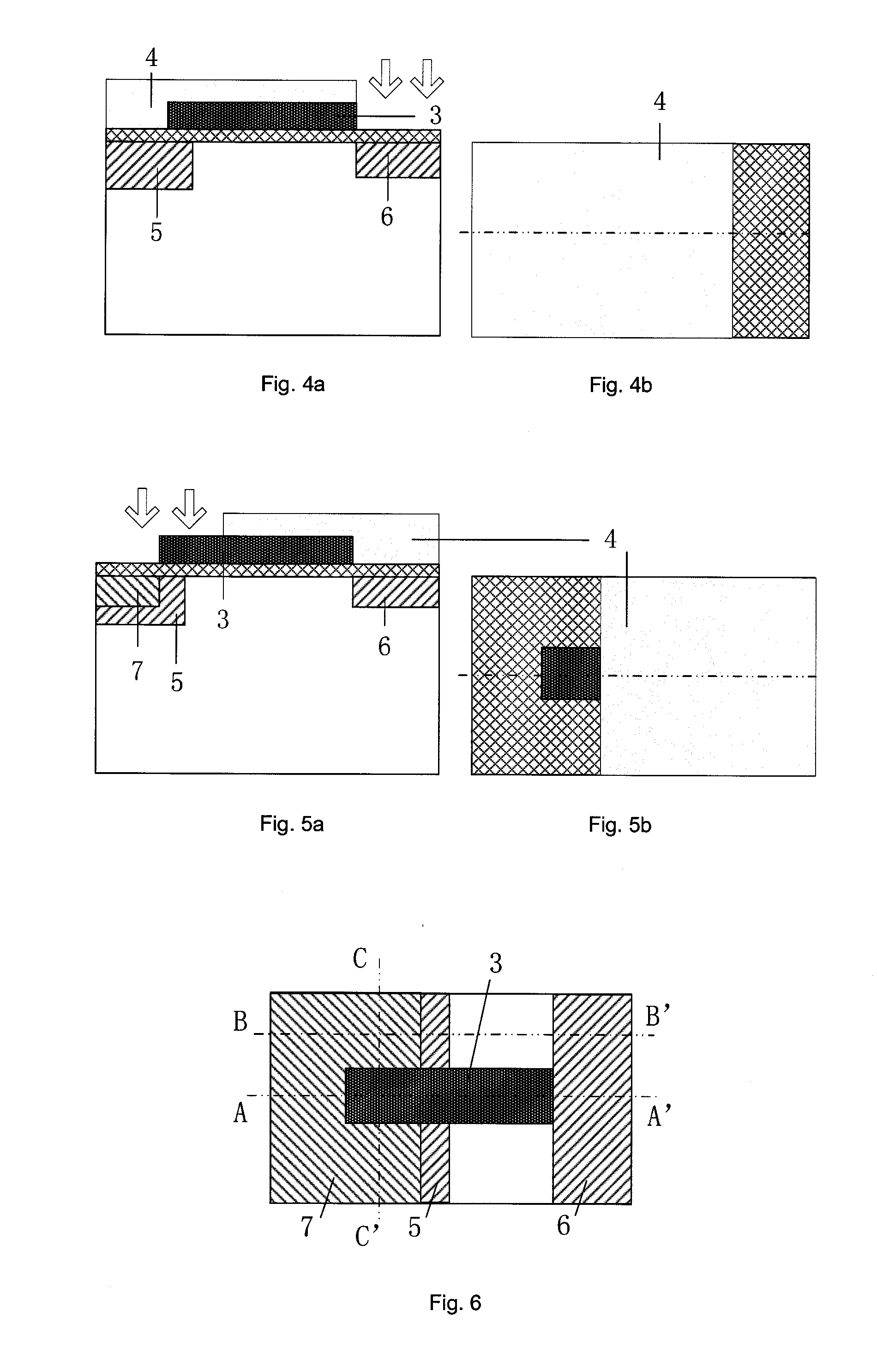
[0036]A specific example of the preparation method according to the present invention includes the process steps shown in FIG. 1 to FIG. 5b:

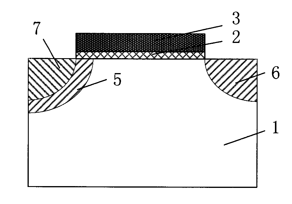
[0037]1. forming an active region isolation layer on a silicon substrate 1 of a bulk silicon wafer with a crystal orientation (100) by using a shallow trench isolation technology, the substrate having a lightly-doped doping concentration; then thermally growing a ga...


PUM


Abstract

The present invention discloses a strip-shaped gate-modulated tunneling field effect transistor with double-diffusion and a preparation method thereof, belonging to a field of CMOS field effect transistor logic device and the circuit. The tunneling field effect transistor includes a semiconductor substrate, a highly-doped source region, a highly-doped drain region, a double-diffusion source region, a gate dielectric layer, and a control gate, wherein the control gate has a strip-shaped structure with a gate length greater than a gate width, and at one side thereof is connected to the highly-doped drain region and at the other side thereof extends laterally into the highly-doped source region; a region located below the control gate is a channel region; the gate width of the control gate is less than twice width of a source depletion layer; the double-diffusion region has the same doping region as the highly-doped source region and the double-diffusion region has the same doping type as the highly-doped drain region; and the channel region located below a portion of the control gate portion in the highly-doped source region has double-diffusion source doped impurities. The TFET device according to the invention improves its performance, and the preparation method thereof is simple.

Description

[0001]The present application claims priority of Chinese Patent Application (No. 201210501691.4), filed on Nov. 29, 2012, which is incorporated herein by reference in its entirety.TECHNICAL FIELD[0002]The invention belongs to a field of a field effect transistor logic device and a circuit in CMOS ultra large scale integrated circuit (ULSI), and particularly refers to a strip-shaped gate tunneling field effect transistor with double-diffusion and a preparation method thereof.BACKGROUND OF THE INVENTION[0003]Under the drive of Moore's Law, the feature size of the conventional MOSFET continues to shrink, now has to enter the nanometer scale, consequently, the negative effects such as short channel effect of a device and so on have become more serious. The effects of drain induced barrier lowering, band-to-band tunneling and so on cause a off-state leakage current of a device to increase continually, at the same time, a sub-threshold slope of the conventional MOSFET can not decrease syn...

Claims


Application Information

Patent Timeline
Patent Type & Authority Applications(United States)
IPC IPC(8): H01L29/423H01L21/324H01L21/28H01L21/266H01L29/78H01L29/66
CPCH01L29/42376H01L29/7816H01L29/66681H01L29/7311H01L21/266H01L21/324H01L21/28114H01L29/66356H01L29/7391
Inventor HUANG, RUHUANG, QIANQIANQIU, YINGXINZHAN, ZHANWANG, YANGYUAN
Owner PEKING UNIV
Why Eureka
Try Eureka