Tunnel Field Effect Transistor and Manufacturing Method

A technique of tunneling field effect and manufacturing method, which is applied in the field of tunneling field effect transistors and its manufacturing, can solve problems such as inability to manufacture logic circuits, difficulty in wide-scale application, and increased resistance value, and achieve large tunneling area and strong Spin-orbit coupling, performance-enhancing effect

Active Publication Date: 2018-10-16
SEMICON MFG INT (SHANGHAI) CORP
View PDF3 Cites 0 Cited by
  • Summary
  • Abstract
  • Description
  • Claims
  • Application Information

AI Technical Summary

Problems solved by technology

This structure lacks carriers, resulting in a sharp increase in resistance, and the absence of a band gap means that logic circuits that must perform switching operations cannot be fabricated
Therefore, graphene is still difficult to be widely used in semiconductor manufacturing

Method used


Image

  • Tunnel Field Effect Transistor and Manufacturing Method
  • Tunnel Field Effect Transistor and Manufacturing Method
  • Tunnel Field Effect Transistor and Manufacturing Method

Examples


Embodiment Construction

[0045] In order to further improve the performance of the existing tunneling field-effect transistor (The tunneling field-effect transistor, TFET), the present invention provides a manufacturing method of the tunneling field-effect transistor, comprising:

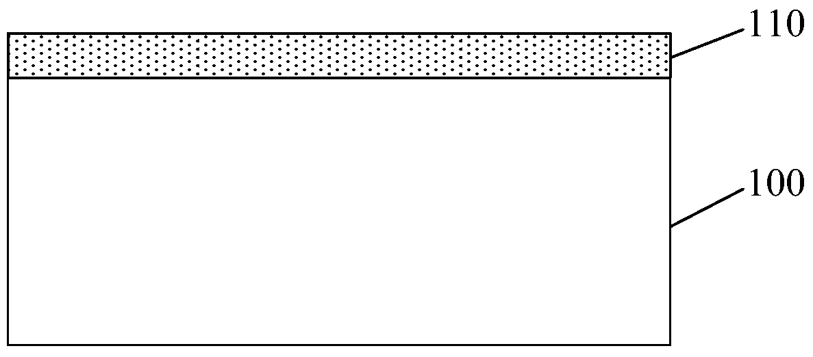
[0046] provide the substrate;

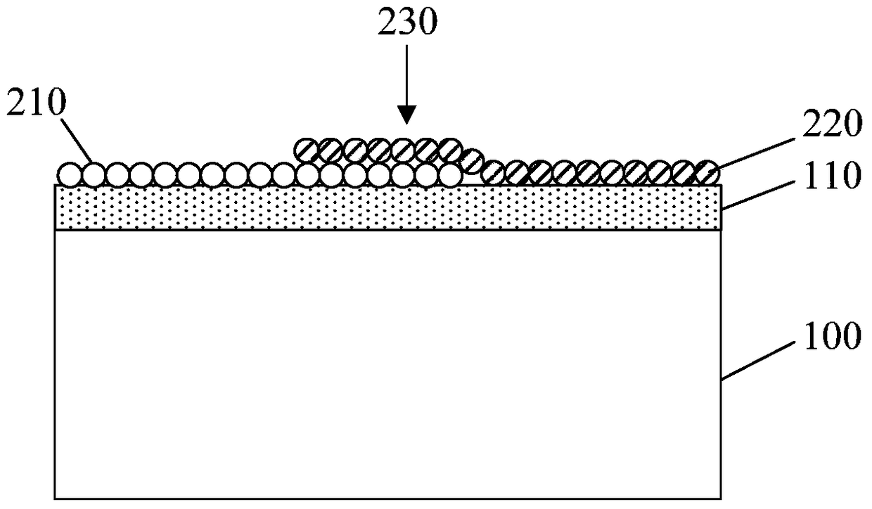
[0047] forming a P-type silicene layer and an N-type silicene layer on the substrate, so that the P-type silicene layer and the N-type silicene layer overlap and contact each other at the junction of the two to form a laminated structure;

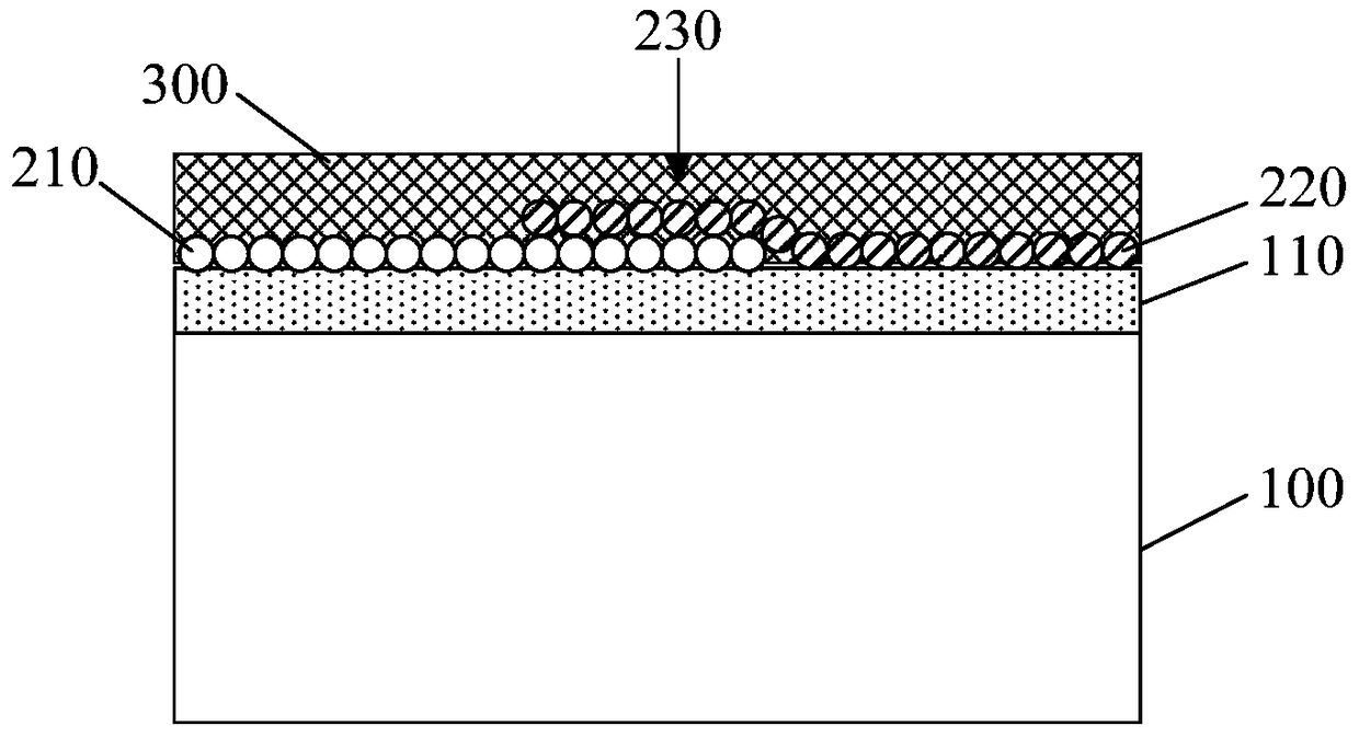
[0048] forming a gate structure on the stacked structure;

[0049] Electrodes are respectively formed on the P-type silicene layer and the N-type silicene layer on both sides of the gate structure to form a source or drain with the P-type silicene layer and the N-type silicene layer.

[0050] Through the above steps to form a tunnel field effect transistor, in which silicene has higher electron mobility and stronger spin-orbit coupling, so it can open a l...


PUM


Abstract

The present invention provides a tunnel field effect transistor and a manufacturing method thereof. The tunnel field effect transistor comprises a substrate; a P-type silylene layer and an N-type silylene layer which form a lamination structure; a grid structure located on the lamination structure; electrodes located on the P-type silylene layer and the N-type silylene layer at the two sides of the grid structure and used for forming a source or a drain with the P-type silylene layer and the N-type silylene layer. The present invention also provides a manufacturing method of the tunnel field effect transistor. The manufacturing method of the tunnel field effect transistor comprises the steps of providing the substrate; forming the P-type silylene layer and the N-type silylene layer to thereby enable the P-type silylene layer and the N-type silylene layer to overlap and contact at the intersection position mutually to form the lamination structure; forming the grid structure on the lamination structure; forming the electrodes on the P-type silylene layer and the N-type silylene layer at the two sides of the grid structure, wherein the electrodes are used to form the source or drain with the P-type silylene layer and the N-type silylene layer. The tunnel field effect transistor of the present invention has a larger tunneling area, and enables the performance to be improved to a certain extent.

Description

technical field [0001] The invention relates to the field of semiconductor manufacturing, in particular to a tunnel field effect transistor and a manufacturing method thereof. Background technique [0002] In order to meet the increasing performance requirements for semiconductor devices, new technologies have been developed in the field of semiconductor manufacturing to obtain more ideal performance. For example, the tunneling field-effect transistor (TFET) has begun to partially Replace the existing metal oxide semiconductor field effect transistor (Metal Oxide Semiconductor Field Effect Transistor, MOSFET). [0003] In a conventional tunnel field effect transistor, a gate and source and drain regions are formed on a low-doped intrinsic semiconductor material substrate. When a voltage is applied to the gate, an electron accumulation layer and a depletion layer are formed on the surface of the channel region under the gate, the electron energy band bends downward, and the ...

Claims


Application Information

Patent Timeline
Patent Type & Authority Patents(China)
IPC IPC(8): H01L29/739H01L29/06H01L29/16H01L21/331
Inventor 肖德元
Owner SEMICON MFG INT (SHANGHAI) CORP
Why Eureka
Try Eureka