Tunneling Field Effect Transistor and Method of Forming the Same

A tunneling field effect, transistor technology, applied in semiconductor devices, semiconductor/solid-state device manufacturing, electrical components, etc., can solve the problems of sub-threshold swing reduction, low drive current, small on-state current, etc., to increase tunneling Area, increased tunneling path, effect of increased length

Active Publication Date: 2017-11-03
SEMICON MFG INT (SHANGHAI) CORP
View PDF5 Cites 0 Cited by
  • Summary
  • Abstract
  • Description
  • Claims
  • Application Information

AI Technical Summary

Problems solved by technology

[0004] However, the existing tunneling field effect transistors are limited by the tunneling probability of the source junction and the tunneling area, which faces the problems of small on-state current and reduced sub-threshold swing.
Although new tunneling field-effect transistor implementations have been proposed, such as green FETs, high drive currents and Swings below 60mV / dec have never been achieved
In conclusion, although the simulation results of tunneling field effect transistors are very attractive, due to the low drive current (drive current) and the degraded subthreshold swing (subthreshold swing), the experimental results of tunneling field effect transistors cannot be compared with traditional Metal-Oxide-Semiconductor Field-Effect Transistor (MOSFET) Competition
[0005] To this end, a new tunneling field effect transistor and its preparation method are needed to solve the problems of small on-state current and subthreshold swing of tunneling field effect transistors.

Method used


Image

  • Tunneling Field Effect Transistor and Method of Forming the Same
  • Tunneling Field Effect Transistor and Method of Forming the Same
  • Tunneling Field Effect Transistor and Method of Forming the Same

Examples


Embodiment Construction

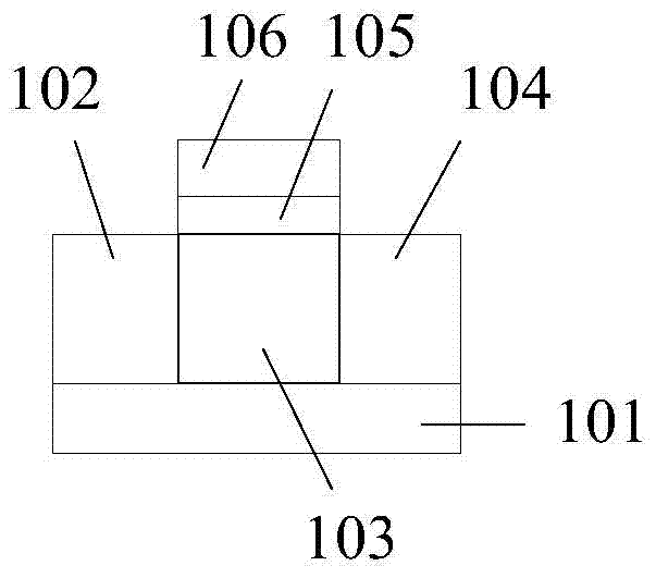
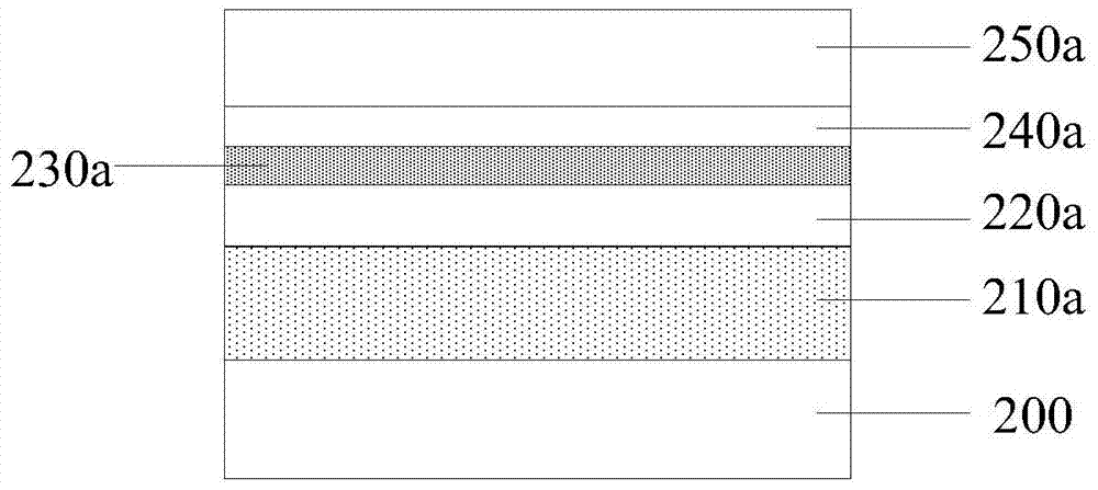
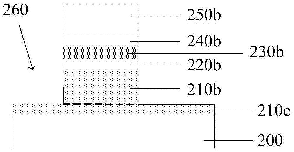
[0055] Existing tunneling field effect transistors cannot achieve high on-state current and low sub-threshold slope, and the tunneling path and tunneling area are the most important factors that determine the performance of tunneling field effect transistors. The long tunneling path and larger tunneling area help to improve the performance of tunneling field effect transistors.

[0056] To this end, the present invention provides a new tunneling field effect transistor having a second channel region surrounding the first doped region, the first channel region and the second doped region at the same time. Since the length of the second channel region is significantly increased, the tunneling path of the transistor is increased, and because the second channel region completely covers the first doped region and the side surfaces of the first channel region, and at least covers the second doped region Therefore, the area of ​​the second channel region is larger, which increases the t...


PUM


Abstract

A tunneling field effect transistor and its forming method, the tunneling field effect transistor comprising: a semiconductor substrate; a first semiconductor layer on the semiconductor substrate, the first semiconductor layer has a first doping type ; an annular groove located in the first semiconductor layer; a first doped region located on the first semiconductor layer and surrounded by the annular groove, the first doped region having a first doping type ; a first channel region located on the first doped region; a second doped region located on the first channel region, the second doped region having a second doping type; The second doped region, the first channel region, the side of the first doped region and the second channel region at the bottom of the annular groove; the gate located in the annular groove; the gate located in the second channel The gate dielectric layer between the region and the gate. Both the tunneling path and the tunneling area of ​​the tunneling field effect transistor are increased, so the performance of the tunneling field effect transistor is improved.

Description

Technical field [0001] The invention relates to the field of semiconductor manufacturing, in particular to a tunneling field effect transistor and a method for forming the same. Background technique [0002] In order to be able to apply semiconductor devices in the field of ultra-low voltage and low power consumption, device structures and process preparation methods that use a new type of conduction mechanism to obtain an ultra-steep sub-threshold slope have become the focus of attention in small-sized devices. In recent years, researchers have proposed a possible solution, which is to use tunnel field effect transistors (TFET). Tunneling field effect transistors are different from traditional metal-oxide-semiconductor field effect transistors (MOSFET). The source and drain doping types of tunneling field effect transistors are opposite. The gate is used to control the band-band of the reverse-biased PIN junction. Tunneling realizes conduction, which can break through the 60mV / ...

Claims


Application Information

Patent Timeline
Patent Type & Authority Patents(China)
IPC IPC(8): H01L29/78H01L29/08H01L21/336
Inventor 陈勇
Owner SEMICON MFG INT (SHANGHAI) CORP
Why Eureka
Try Eureka