Thin-film piezoelectric element, thin-film piezoelectric actuator, thin-film piezoelectric sensor, hard disk drive, and inkjet printer apparatus

a piezoelectric actuator and actuator technology, applied in the direction of inking apparatus, device material selection, instruments, etc., can solve the problems of high dielectric loss and material cannot provide piezoelectric performance, and achieve the effect of reducing the effect of environmental and human body, reducing the dielectric loss, and improving reliability

Active Publication Date: 2014-05-29
TDK CORPARATION
View PDF1 Cites 11 Cited by
  • Summary
  • Abstract
  • Description
  • Claims
  • Application Information

AI Technical Summary

Benefits of technology

[0030]The thin-film piezoelectric element according to the present invention has lower dielectric loss than conventional thin-film piezoelectric elements. Thus, in the thin-film piezoelectric element, the thin-film piezoelectric actuator, the thin-film piezoelectric sensor, the hard disk drive, and the ink jet printer apparatus according to the present invention, operation failure is not caused by heat generation during operation, thereby improving reliability.
[0031]The thin-film piezoelectric element according to the present invention has low dielectric loss in a high frequency region and can be applied to a high-frequency element.
[0032]The piezoelectric thin film according to the present invention is a lead-free piezoelectric material, thus reducing the effect on the environment and the human body. Hence, the thin-film piezoelectric element, the thin-film piezoelectric actuator, the thin-film piezoelectric sensor, the hard disk drive, and the ink jet printer apparatus according to the present invention can be applied to applications where the use of conventional thin-film piezoelectric elements is difficult.

Problems solved by technology

However, this material has high dielectric loss, so the material cannot provide the piezoelectric performance, depending on a frequency used.

Method used


Image

  • Thin-film piezoelectric element, thin-film piezoelectric actuator, thin-film piezoelectric sensor, hard disk drive, and inkjet printer apparatus
  • Thin-film piezoelectric element, thin-film piezoelectric actuator, thin-film piezoelectric sensor, hard disk drive, and inkjet printer apparatus
  • Thin-film piezoelectric element, thin-film piezoelectric actuator, thin-film piezoelectric sensor, hard disk drive, and inkjet printer apparatus

Examples


example 1

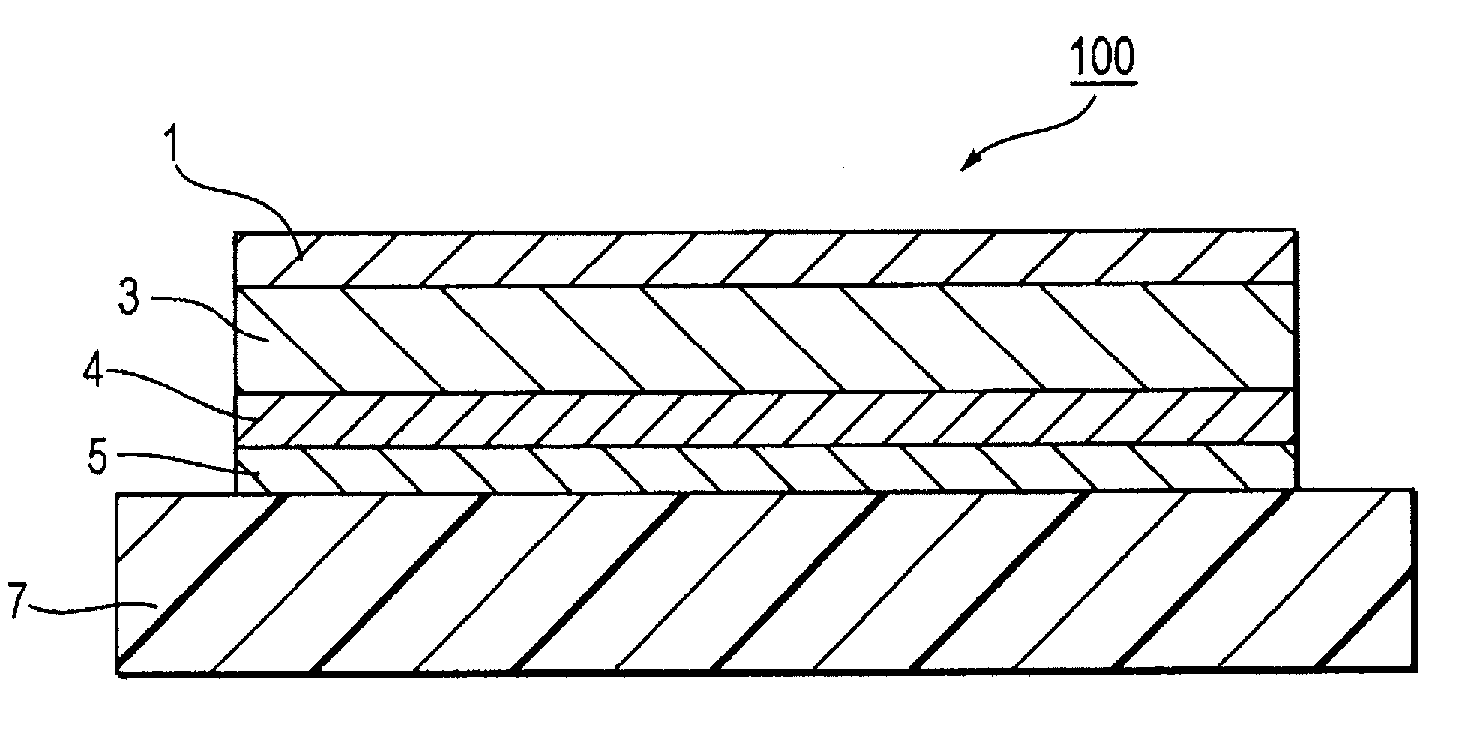
[0099]The thin-film piezoelectric element 100 according to Example 1 was produced as described below.

[0100]The silicon (100) substrate 7 was heated to 400° C. Pt was epitaxially grown by a sputtering method on the silicon substrate 7 to form a 200-nm-thick Pt film serving as the first electrode film 5 in such a manner that the Pt film was oriented to the plane of the silicon substrate 7. In this case, the deposition rate was 0.2 nm / sec.

[0101]Next, the silicon substrate 7 was heated to 550° C. The piezoelectric thin film 3 was epitaxially grown by a sputtering method so as to have a thickness of 2000 nm. In this case, a sintered compact having a composition of (K0.17Na0.76Sr0.07)0.96(Nb0.9Zr0.1)O3 was used as a sputtering target for the piezoelectric thin film 3. The film composition of the piezoelectric thin film 3 was almost the same as the target composition.

[0102]Next, a Pt film having a thickness of 200 nm was formed as the second electrode film 1 by a sputtering method at room ...

examples 10 to 12

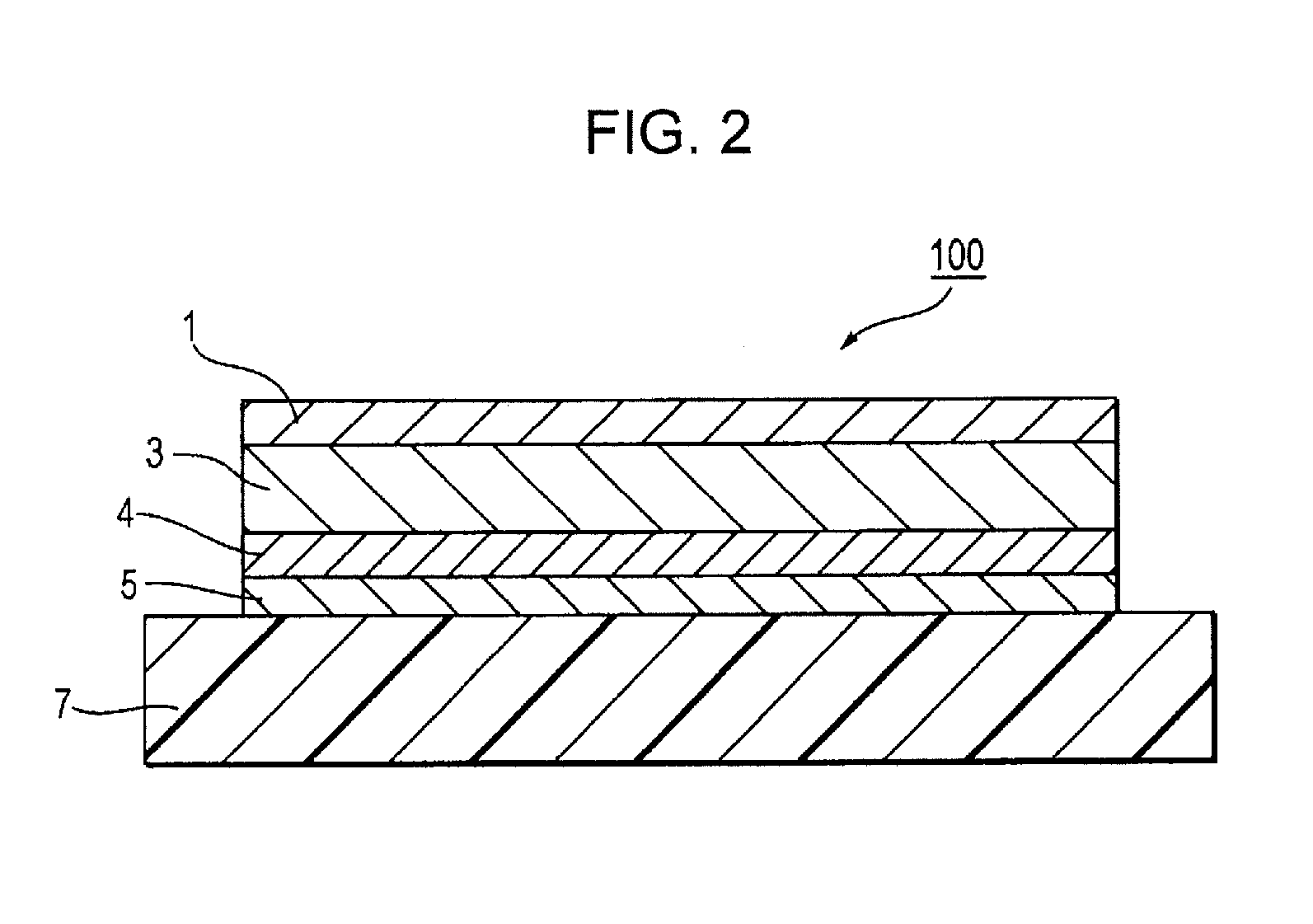
[0105]As with Example 1, each silicon substrate 7 was heated to 400° C. Pt was epitaxially grown by a sputtering method on the silicon substrate 7 to form a 200-nm-thick Pt film serving as the first electrode film 5 in such a manner that the Pt film was oriented to the plane of the silicon substrate 7. A 35-nm-thick strontium ruthenate SrRuO3 film serving as the intermediate film 4 was formed by a sputtering method on the first electrode film 5.

[0106]In Example 10, a sputtering target containing materials described in Table 1 was used for the piezoelectric thin film 3. In Example 11, as described in Table 1, a sputtering target further containing 0.11 at % Ba and 6.5 at % Ta was used. In Example 12, as described in Table 1, a sputtering target further containing 0.11 at % Ba, 6.5 at % Ta, and 0.35 at % Mn was used. Here, the elements were contained in such a manner that the total content of the elements in the entire piezoelectric thin film containing the elements was 100 at %. Ther...


PUM


Abstract

There are provided a thin-film piezoelectric element including a piezoelectric thin film which has an alkali niobate-based perovskite structure represented by the composition formula (K1-w-xNawSrx)m(Nb1-yZry)O3 and which is preferentially oriented to (001), and a pair of electrode films that sandwich the piezoelectric thin film, a thin-film piezoelectric actuator, and a thin-film piezoelectric sensor each including the thin-film piezoelectric element.

Description

[0001]This is a Continuation-in-Part of application Ser. No. 13 / 687,786 filed Nov. 28, 2012. The disclosure of the prior application is hereby incorporated by reference herein in its entirety.BACKGROUND OF THE INVENTION[0002]1. Field of the Invention[0003]The present invention relates to a thin-film piezoelectric element composed of a thin-film piezoelectric material; a thin-film piezoelectric actuator and a thin-film piezoelectric sensor that include the thin-film piezoelectric elements; and a hard disk drive and an ink jet printer apparatus that include the thin-film piezoelectric actuators.[0004]2. Related Background Art[0005]In recent years, there have been advances in practical use of thin-film piezoelectric elements including thin-film piezoelectric materials, instead of bulk piezoelectric materials. Examples thereof include gyroscope sensors, pressure sensors, pulse wave sensors, shock sensors, and microphones, which use a piezoelectric effect, in which a force applied to a p...

Claims


Application Information

Patent Timeline
Patent Type & Authority Applications(United States)
IPC IPC(8): H01L41/18
CPCB41J2/14233G01C19/5621G01L9/008G11B5/5552B41J2202/03G11B5/483A61B5/02444H10N30/10516H10N30/8542H10N30/076
Inventor KURACHI, KATSUYUKIAIDA, YASUHIROSAKUMA, HITOSHIMAEJIMA, KAZUHIKO
Owner TDK CORPARATION
Why Eureka
Try Eureka