Complementary mirror image embedded planar resistor architecture

a technology of embedded planar resistors and mirror images, which is applied in the association of printed resistors, non-printed electrical components of printed circuits, electrical apparatus construction details, etc., can solve the problems of deepening the influence of parasitic effects, impedance drops, and inability to meet high frequency application requirements, so as to reduce parasitic capacitance and efficiently enhance the application frequency range

Active Publication Date: 2008-04-24
IND TECH RES INST
View PDF16 Cites 9 Cited by
  • Summary
  • Abstract
  • Description
  • Claims
  • Application Information

AI Technical Summary

Benefits of technology

[0009]The present invention is directed to providing a complementary mirror image embedded planar resistor architecture. A hollow structure is formed in a ground plane or in an electrode, both of which are adjacent to the embe

Problems solved by technology

Furthermore, the higher the frequency is, the deeper the influence of the parasitic effects is.
It can be seen from FIG. 1C that, when the frequency becomes higher, due to the ground plane below the embedded planar resistor, t

Method used


Image

  • Complementary mirror image embedded planar resistor architecture
  • Complementary mirror image embedded planar resistor architecture
  • Complementary mirror image embedded planar resistor architecture

Examples


Embodiment Construction

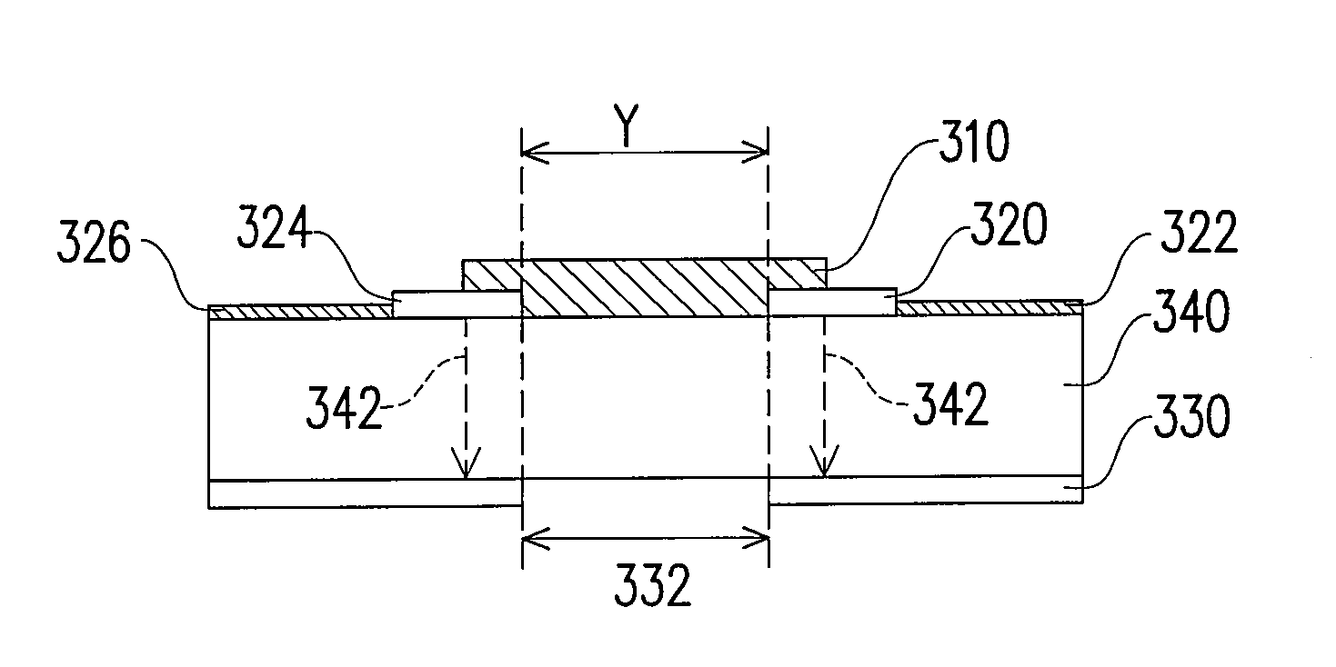
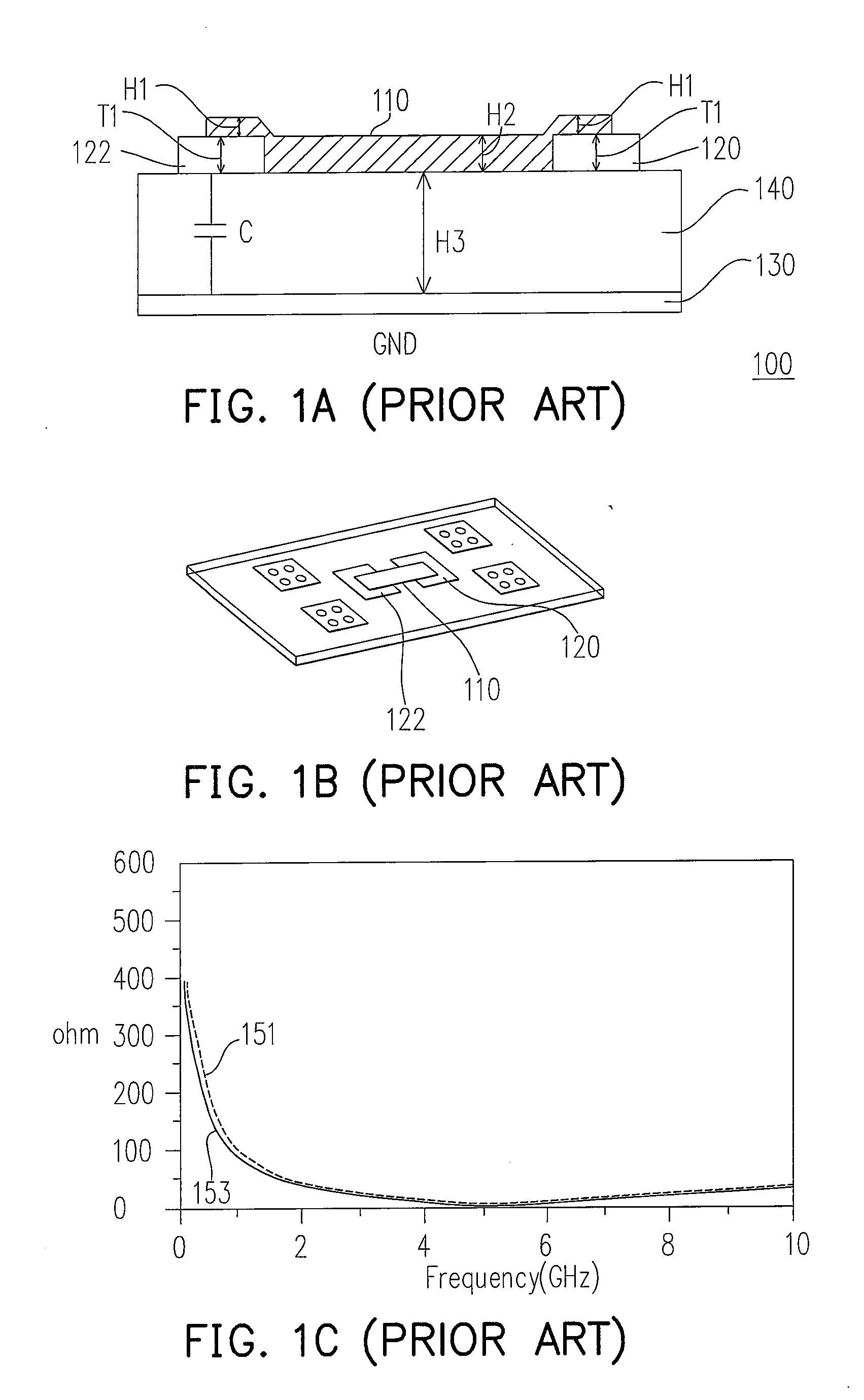
[0042]The design of an embedded planar resistor usually presents different electrical characteristics due to the effects of the parasitic components generated between the embedded resistor and the conductive layer, such as a metal ground plane, an electrode layer, or a power supply layer. The higher the frequency is, the greater the influence of the parasitic effects is. On the other hands, when other signal transmission lines pass through, if there is no shield at all, serious interference or cross talk phenomenon occurs. In the present invention, the design of the structure between the embedded planar resistor and a ground plane or an electrode layer or a power supply layer is improved, so as to increase the application frequency, thus, the embedded planar resistor is more suitable for a high frequency application circuit.

[0043]In order to enhance the aforementioned characteristics, a novel structure must be designed to achieve the high frequency application. As for the design of ...


PUM


Abstract

A complementary mirror image embedded planar resistor architecture is provided. In the architecture, a complementary hollow structure is formed on a ground plane or an electrode plane to minimize the parasitic resistance, so as to efficiently enhance the application frequency. In addition, in some cases, some signal transmission lines pass through the position below the embedded planar resistor, and if there is no shield at all, serious interference or cross talk phenomenon occurs. Therefore, the complementary hollow structure of the ground plane, the electrode plane, or a power layer adjacent to the embedded planar resistor is designed to be a mesh structure, so as to reduce the interference or cross talk phenomenon. In this manner, the whole resistor structure has preferable high frequency electrical characteristic in the circuit.

Description

CROSS-REFERENCE TO RELATED APPLICATION[0001]This application claims the priority benefit of Taiwan application serial no. 95138693, filed Oct. 20, 2006. All disclosure of the Taiwan application is incorporated herein by reference.BACKGROUND OF THE INVENTION[0002]1. Field of Invention[0003]The present invention relates to a design of an embedded planar resistor in a multi-layer circuit substrate, and more particularly, to a complementary mirror image embedded planar resistor architecture, in which a complementary hollow structure is formed on a ground plane or an electrode plane adjacent to the embedded planar resistor.[0004]2. Description of Related Art[0005]High frequency, broadband, and miniaturization have almost become the greatest requirements for high-tech industries and markets, such as wireless communication, digital computers, portable electronic products, and information house appliances. Under the trend of using an embedded component to reduce the area of a circuit, gener...

Claims


Application Information

Patent Timeline
IPC IPC(8): H05K1/16
CPCH05K1/0224H05K1/025H05K1/0298H05K2201/0969H05K2201/0792H05K2201/09681H05K1/167
Inventor JOW, UEI-MINGLEE, MIN-LINLAY, SHINN-JUHSHYU, CHIN-SUNCHEN, CHANG-SHENGLAI, YING-JIUNN
Owner IND TECH RES INST
Why Eureka
Try Eureka