
Liquid crystal phase shifter, liquid crystal antenna and manufacturing method of liquid crystal phase shifter

a technology of phase shifter and liquid crystal, which is applied in the direction of antennas, instruments, electrical equipment, etc., can solve the problems of reducing the performance of the antenna, reducing the dielectric loss, and poor signals,

Active Publication Date: 2022-07-26
TRUWIN OPTO ELECTRONICS LTD
View PDF11 Cites 0 Cited by
  • Summary
  • Abstract
  • Description
  • Claims
  • Application Information

AI Technical Summary

Benefits of technology

[0034]Compared with the prior art, the present disclosure has the following beneficial effects.
[0035]1. In ultra-high-frequency wireless communications, the larger a dielectric constant and a dielectric loss value of a substrate material are, the higher the dielectric loss is, and the poorer signals are. The PCBs used in the present application are used as the substrates of the liquid crystal antenna. The dielectric constants and the dielectric loss of the PCBs are less than those of a glass substrate usually used by a liquid crystal panel, so that the PCBs are lower in dielectric loss, which is favorable for improving the performance of the liquid crystal antenna in ultra-high frequency band application.
[0036]2. Further, since the PCBs are non-transparent, it is not favorable for the oppositely bonding of the two substrates by using a transparent mark capturing method, causing a failure of accurate alignment, which cannot meet the design requirements of the antenna and then greatly reduces the performance of the antenna. In the present application, the alignment marks are further respectively disposed on the first metal film layer and the second metal film layer, and the through holes corresponding to the alignment marks in position are respectively disposed in the first substrate and the second substrate, so that the two substrates can be oppositely bonded by using the transparent mark capturing after the improvement.
[0037]3. Furthermore, in order to simplify the flow and the process, the alignment marks are the metal alignment marks obtained by performing exposure and etching on the corresponding metal film layers. The size of the metal alignment marks is smaller than that of the through holes. By disposing the transparent carrier layers between the metal film layers and the corresponding substrates, the metal alignment marks obtained by the exposure and etching can be supported, and the transparent carrier layers cannot affect the transparent mark capturing based oppositely bonding.

Problems solved by technology

How to design and manufacture a liquid crystal phase shifter and a liquid crystal antenna suitable for the spectrums above the ultra-high frequency bands is a problem to be solved by those skilled in the art.
1. In ultra-high-frequency wireless communications, the larger a dielectric constant and a dielectric loss value of a substrate material are, the higher the dielectric loss is, and the poorer signals are.
2. Further, since the PCBs are non-transparent, it is not favorable for the oppositely bonding of the two substrates by using a transparent mark capturing method, causing a failure of accurate alignment, which cannot meet the design requirements of the antenna and then greatly reduces the performance of the antenna.

Method used


Image

  • Liquid crystal phase shifter, liquid crystal antenna and manufacturing method of liquid crystal phase shifter
  • Liquid crystal phase shifter, liquid crystal antenna and manufacturing method of liquid crystal phase shifter
  • Liquid crystal phase shifter, liquid crystal antenna and manufacturing method of liquid crystal phase shifter

Examples


embodiment i

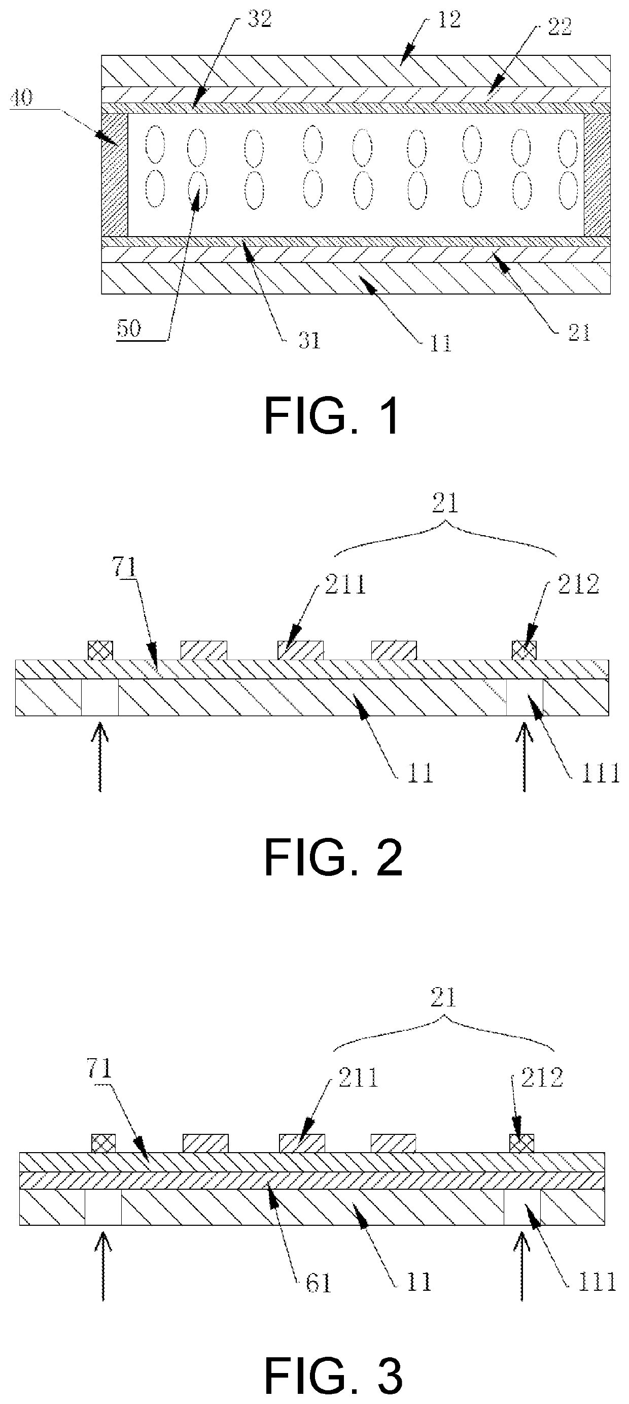
[0049]As shown in FIG. 1, illustrating Embodiment I of the present disclosure, the present specific embodiment provides a liquid crystal phase shifter. The liquid crystal phase shifter includes a first substrate 11 and a second substrate 12 which are disposed oppositely, and further includes a liquid crystal layer 50 located between the first substrate 11 and the second substrate 12.

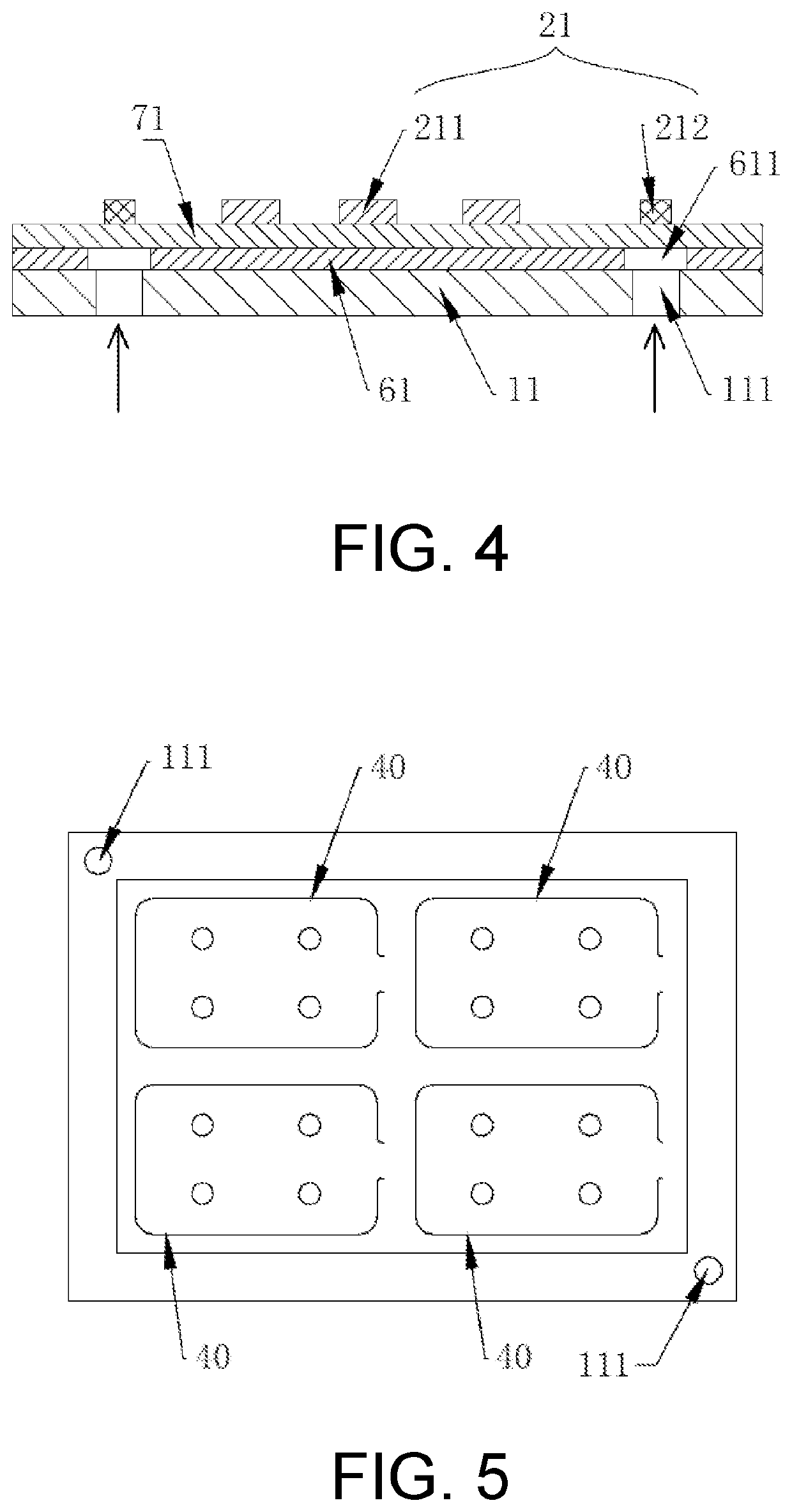
[0050]Sealant 40 is further disposed between the first substrate 11 and the second substrate 12. The sealant 40 is located at the edges of the first substrate 11 and the second substrate 12, and is used for sealing the liquid crystal layer 50. Preferably, supports containing plastic balls and the epoxy sealant 40 are distributed in the liquid crystal layer 50.

[0051]The first substrate 11 is provided with a first conductive layer, and the second substrate 12 is provided with a second conductive layer.

[0052]The side of the first substrate 11 facing the second substrate 12 is provided with a first metal fil...

embodiment ii

[0092]The present specific embodiment provides a liquid crystal antenna. The liquid crystal antenna includes the liquid crystal phase shifter in Embodiment I. The liquid crystal antenna further includes an antenna radiation unit used for radiating a microwave signal, thereby realizing feed-in and feed-out of the microwave signal.

[0093]In the present embodiment, the side, away from the second substrate 12, of the first substrate 11 is provided with an antenna radiation unit. The antenna radiation unit is made of a high-conductivity material. The antenna radiation unit may be a rectangular, round, or square patch, may realize corner cutting, and may also be attached to the liquid crystal phase shifter by a patch process. Or, a more preferable solution is that the antenna radiation unit is a patterned third metal film layer disposed on the side, away from the second substrate 12, of the first substrate 11.

embodiment iii

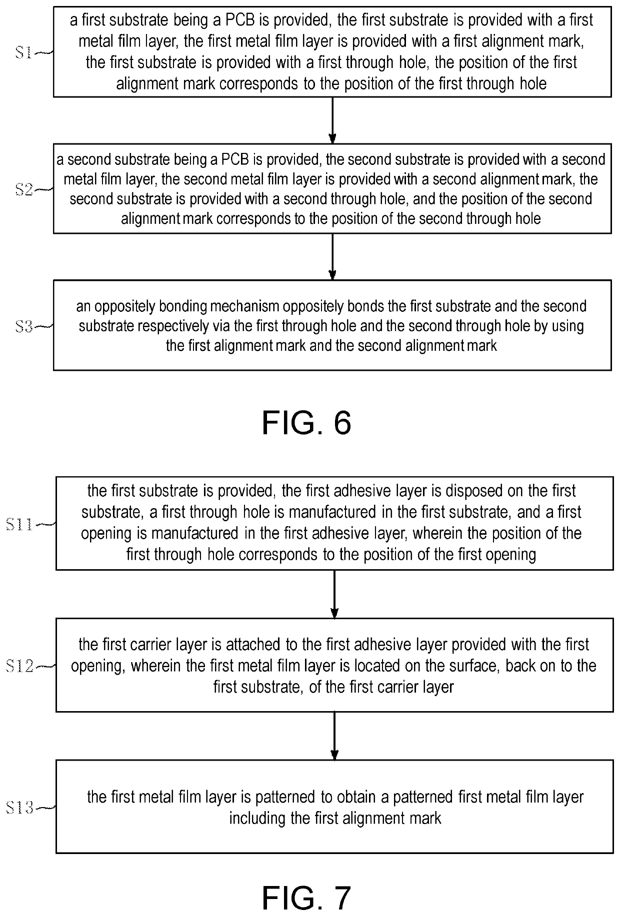
[0094]The present specific embodiment provides a manufacturing method of the liquid crystal phase shifter in Embodiment I. As shown in FIG. 6, the manufacturing method of the liquid crystal phase shifter includes the following steps.

[0095]Step S1: a first substrate 11 being a PCB is provided. The first substrate 11 is provided with a first metal film layer 21.

[0096]The first metal film layer 21 is provided with a first alignment mark 212. The first substrate 11 is provided with a first through hole 111. The position of the first alignment mark 212 corresponds to the position of the first through hole 111.

[0097]Step S2: a second substrate 12 being a PCB is provided. The second substrate 12 is provided with a second metal film layer 22, the second metal film layer 22 is provided with a second alignment mark. The second substrate 12 is provided with a second through hole, and the position of the second alignment mark corresponds to the position of the second through hole.

[0098]Step S3:...


PUM

PropertyMeasurementUnit
frequencyaaaaaaaaaa
thicknessesaaaaaaaaaa
included angleaaaaaaaaaa

Abstract

A liquid crystal phase shifter includes a first substrate and a second substrate which are disposed oppositely, and a liquid crystal layer located between the first substrate and the second substrate. A first metal film layer is disposed on a side of the first substrate facing the second substrate. A second metal film layer is disposed on a side of the second substrate facing the first substrate. The first metal film layer and the second metal film layer are both patterned metal film layers. The first substrate and the second substrate are both PCBs. The present disclosure further provides a liquid crystal antenna, including the abovementioned liquid crystal phase shifter. The present disclosure further provides a manufacturing method of the liquid crystal phase shifter.

Description

CROSS-REFERENCE TO RELATED APPLICATION[0001]This application is a 371 of international application of PCT application serial no. PCT / CN2019 / 082162, filed on Apr. 11, 2019, which claims the priority benefit of China application no. 201910272556.9, filed on Apr. 4, 2019. The entirety of each of the above-mentioned patent applications is hereby incorporated by reference herein and made a part of this specification.BACKGROUNDTechnical Field[0002]The present disclosure relates to the technical field of wireless communications, and more particularly relates to a liquid crystal phase shifter, a liquid crystal antenna and a manufacturing method of the liquid crystal phase shifter.Description of Related Art[0003]The development of information networks is changing rapidly, and major changes are occurring or will occur in various fields. Hotspot technologies include 5G and satellite mobile Internet communication technologies.[0004]As a core device for sending and receiving communication inform...

Claims


Application Information

Patent Timeline
Patent Type & Authority Patents(United States)
IPC IPC(8): H01Q3/36H01P1/18G02F1/13H01P11/00
CPCH01Q3/36G02F1/1313H01P1/184H01P11/00H01P1/18G02F1/1333G02F1/1303H01Q1/38
Inventor LIU, ZHISHENGXU, XIANGZHANWANG, LIXIONGHUANG, YINGQUNWANG, HUXINZAN, DUANQINGHE, JIQIANG
Owner TRUWIN OPTO ELECTRONICS LTD
Learn More