Photocathode Including Silicon Substrate With Boron Layer

Active Publication Date: 2014-02-06
KLA TENCOR CORP
View PDF8 Cites 63 Cited by
  • Summary
  • Abstract
  • Description
  • Claims
  • Application Information

AI Technical Summary

Benefits of technology

The present invention is about a new photocathode structure that solves the problems that previously prevented the commercial use of silicon-based photocathodes. The structure includes a smooth silicon substrate with a high-purity, low-defect layer, and a low work-function layer that effectively creates a negative electron affinity device. Various additional layers can be added to further enhance the beneficial qualities of the photocathode, such as a second boron layer to prevent oxides and defects, an anti-reflective material layer to improve photon capture efficiency, and a metal frame or grid to generate an external potential difference between the illuminated and output surfaces. The sensor can also include an additional boron layer on its receiving surface to improve electron capturing efficiency. Overall, this new photocathode structure solves the problems that previously prevented its commercial use and provides improved performance.

Problems solved by technology

Silicon photocathodes have been made in the past, but have not found significant commercial use because, although silicon is efficient at capturing light, few of the generated electrons are able to escape from the silicon, resulting in low overall efficiency.
Although reflection photocathodes simplify some of the tradeoffs between photocathode thickness and sensitivity that are discussed below, they are not suitable for use in imaging devices such as image intensifiers and EBCCD devices (although they can be suitable for use in some photomultiplier configurations).
Prior-art photocathodes require difficult tradeoffs between conflicting requirements associated with absorbing photons and emitting photoelectrons.
A thicker photocathode increases the probability that an incident photon will be absorbed, but also increases the probability that the resulting emitted photoelectron will recombine (i.e., be lost) before it escapes.
Such a thin photocathode optimized for UV wavelengths will typically have poor sensitivity at visible and infra-red wavelengths as a significant fraction of the incident photons at longer wavelengths will pass through the photocathode without absorption.
Another limitation of prior-art photocathodes is that the energy of the emitted photoelectron varies with the wavelength of absorbed light and may be several eV when a UV photon is absorbed.
However, when an electron undergoes multiple collisions within a photocathode, it is likely to recombine and be lost due to the high level of defects within and / or on the surface of prior-art photocathode materials.
Hence, a reduced energy spread would come at the cost of substantially reduced sensitivity (most incident photons would no longer produce a signal).
One disadvantage of silicon is that silicon has a relatively large work-function (approximately 4.8 eV, Allen and Gobelli, “Work Function, Photoelectric Threshold, and Surface States of Atomically Clean Silicon”, Physical Review vol.
Silicon's relatively large band gap means that thermalized electrons cannot escape from silicon.
Even UV photons absorbed close to the surface of silicon do not create much photocurrent because the photoelectrons do not have enough energy to escape.
A second, more serious, problem with the use of silicon as a photocathode material is that silicon very readily forms a native oxide on its surface.
The interface between silicon and silicon dioxide has defects (due to dangling bonds) where the probability of an electron recombining is very high.
However, even a good quality thermal oxide has a significant defect density at its interface to silicon (typically 109 to 1011 defects per cm2), and the high band gap of the oxide combined with a minimum thickness of close to 2 nm still provides a significant barrier to electrons escaping even if the work-function can be overcome.
For these reasons, silicon has never found significant commercial use as a photocathode.

Method used


Image

  • Photocathode Including Silicon Substrate With Boron Layer
  • Photocathode Including Silicon Substrate With Boron Layer
  • Photocathode Including Silicon Substrate With Boron Layer

Examples


Embodiment Construction

[0038]The present invention relates to an improvement in low light sensors for semiconductor inspection systems. The following description is presented to enable one of ordinary skill in the art to make and use the invention as provided in the context of a particular application and its requirements. As used herein, directional terms such as “top”, “bottom”, “over”, “under”, “upper”, “upward”, “lower”, “down” and “downward” are intended to provide relative positions for purposes of description, and are not intended to designate an absolute frame of reference. Various modifications to the preferred embodiment will be apparent to those with skill in the art, and the general principles defined herein may be applied to other embodiments. Therefore, the present invention is not intended to be limited to the particular embodiments shown and described, but is to be accorded the widest scope consistent with the principles and novel features herein disclosed.

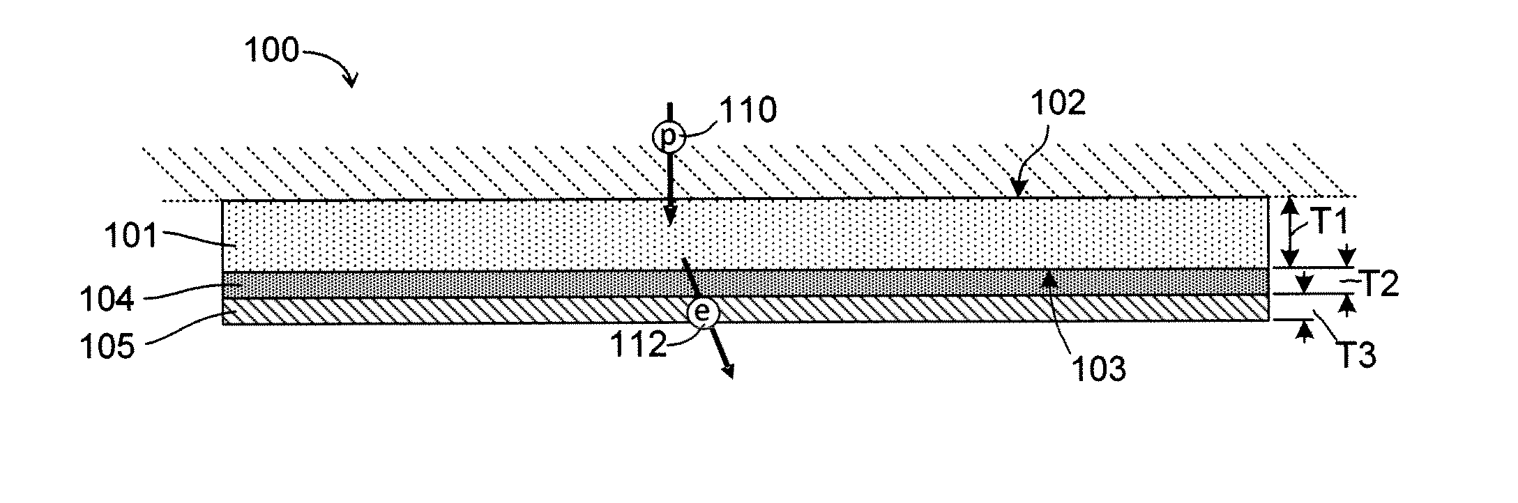
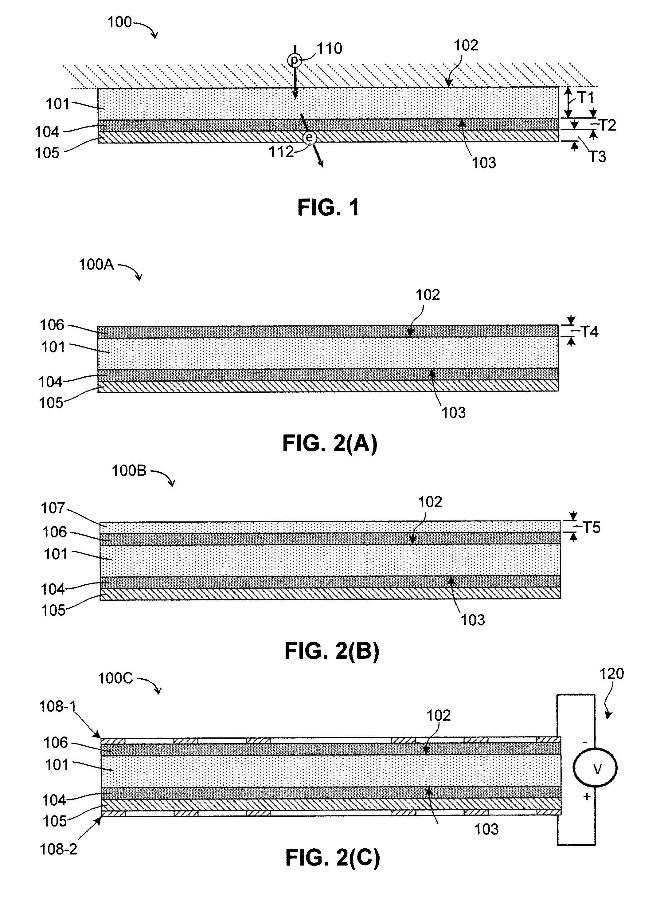
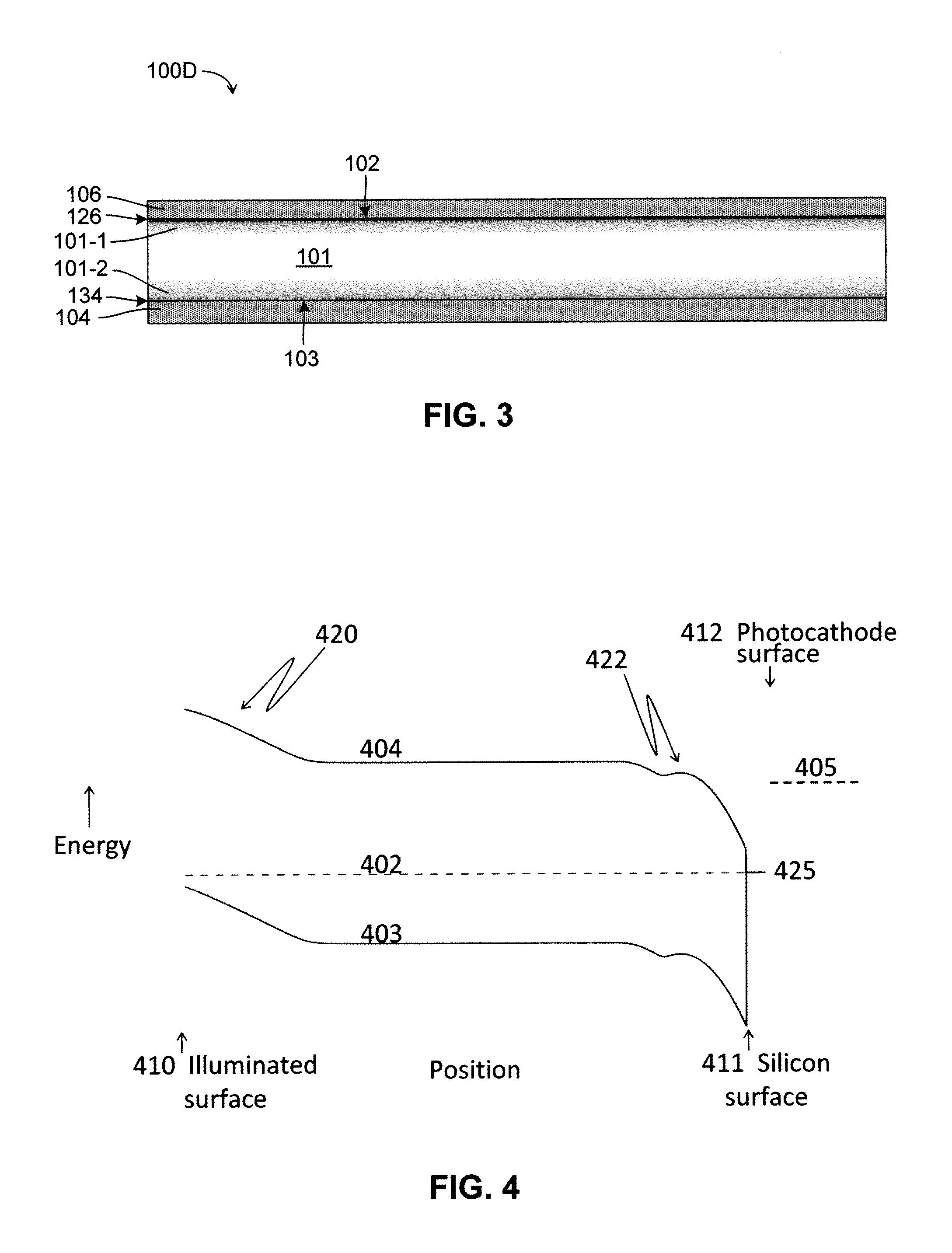
[0039]FIG. 1 illustrates, in cros...


PUM


Abstract

A photocathode is formed on a monocrystalline silicon substrate having opposing illuminated (top) and output (bottom) surfaces. To prevent oxidation of the silicon, a thin (e.g., 1-5 nm) boron layer is disposed directly on the output surface using a process that minimizes oxidation and defects, and a low work-function material layer is then formed over the boron layer to enhance the emission of photoelectrons. The low work-function material includes an alkali metal (e.g., cesium) or an alkali metal oxide. An optional second boron layer is formed on the illuminated (top) surface, and an optional anti-reflective material layer is formed on the boron layer to enhance entry of photons into the silicon substrate. An optional external potential is generated between the opposing illuminated (top) and output (bottom) surfaces. The photocathode forms part of novel sensors and inspection systems.

Description

RELATED APPLICATIONS[0001]This application claims priority to U.S. Provisional Patent Application 61 / 679,200, entitled “Photocathode With Low Noise And High Quantum Efficiency, High Spatial Resolution Low-Noise Image Sensor And Inspection Systems Incorporating an Image Sensor” filed Aug. 3, 2012.BACKGROUND OF THE INVENTION[0002]1. Field of the Invention[0003]The present invention generally relates to low light sensing detectors (sensors) used in conjunction with semiconductor wafer, reticle or photomask inspection systems, and more particularly to photocathodes utilized in the sensors for such inspection systems.[0004]2. Description of the Related Art[0005]Photocathodes are negatively charged electrodes typically used in light detection devices such as photomultipliers, image intensifiers and electron-bombarded CCDs (EBCCDs). Photocathodes comprise a photosensitive compound that, when struck by a quantum of light (photon), generates one (or more) electrons in response to each absorb...

Claims


Application Information

Patent Timeline
IPC IPC(8): H01J29/38
CPCH01J29/385H01J1/34H01J31/26H01J31/50H01L27/14643H01L27/148G02B21/125G01N21/9501H01L27/14806H01L27/14893
Inventor CHUANG, YUNG-HO ALEXFIELDEN, JOHN
Owner KLA TENCOR CORP
Why Eureka
Try Eureka