Method of manufacturing patterned graphene film
a graphene film and patterned technology, applied in the direction of liquid/solution decomposition chemical coating, instruments, photomechanical equipment, etc., can solve the problems of difficult to obtain large-size graphene films, inability to reduce manufacturing costs, and difficulty in controlling the size and thickness of graphene films, etc., to achieve convenient large-scale production, reduce manufacturing costs, and simplify the effect of procedur
- Summary
- Abstract
- Description
- Claims
- Application Information
AI Technical Summary
Benefits of technology
Problems solved by technology
Method used
Image

Examples
example 1
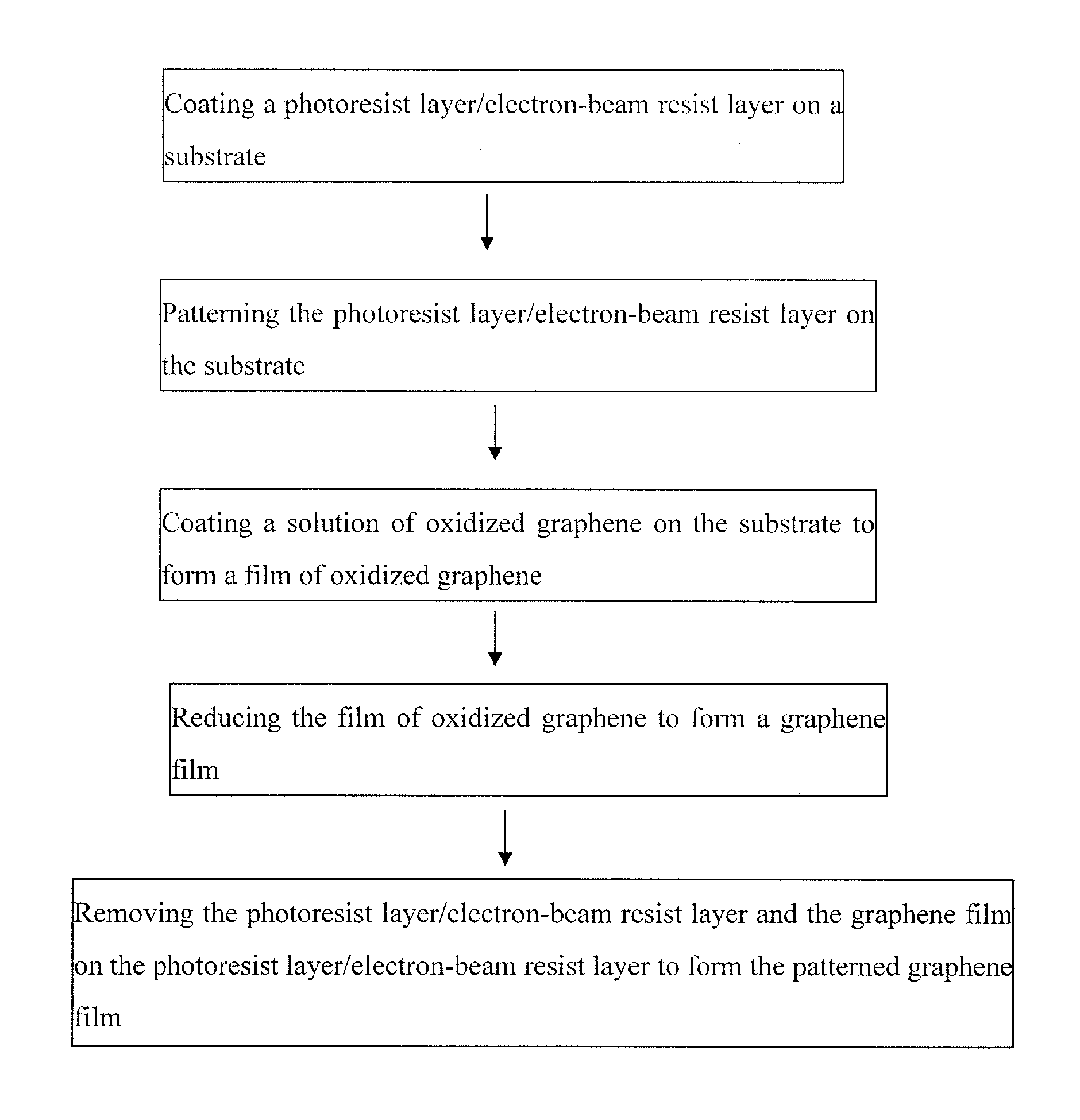
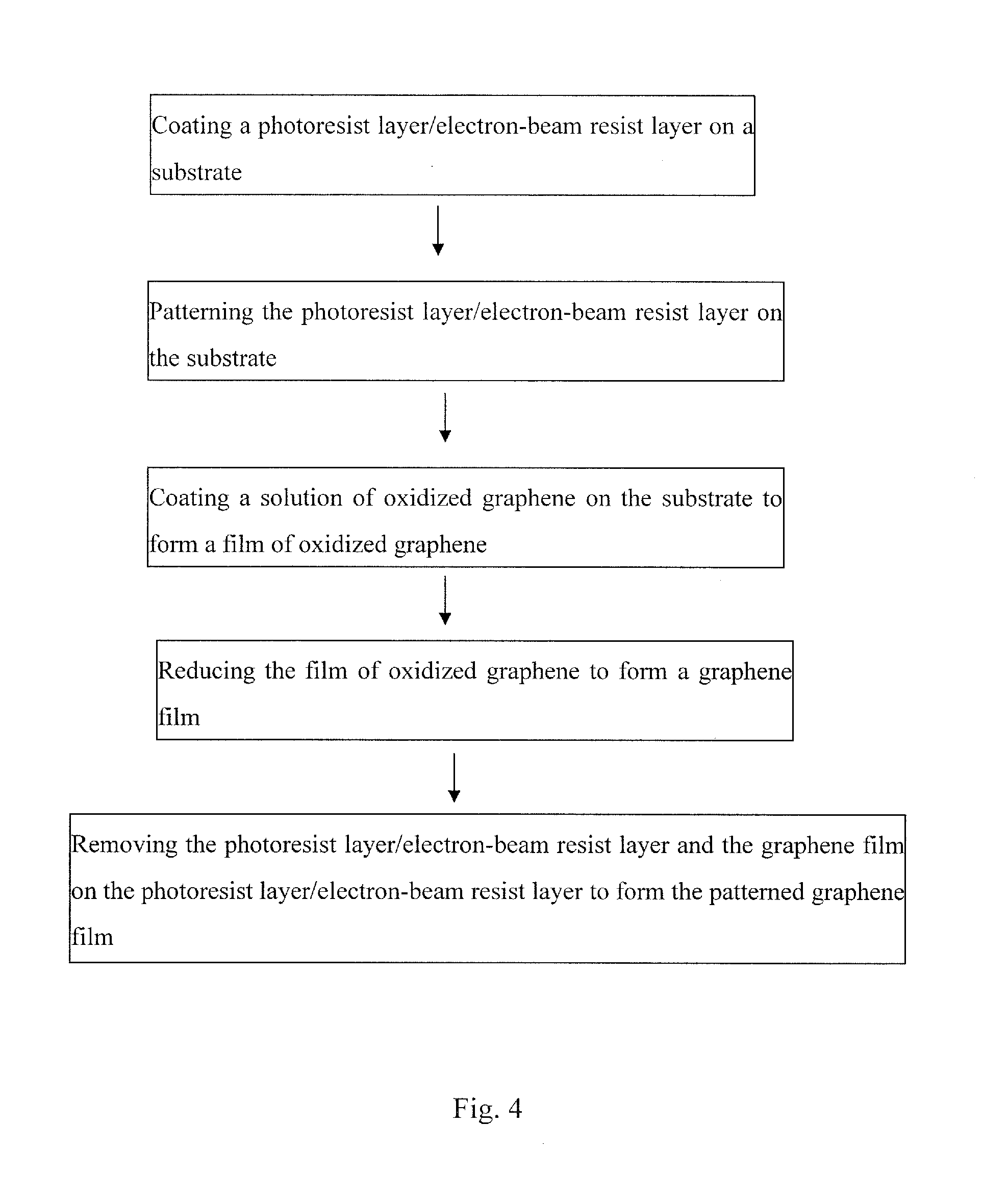
[0033]In the Example 1, the method of manufacturing the patterned graphene film comprises the following steps.
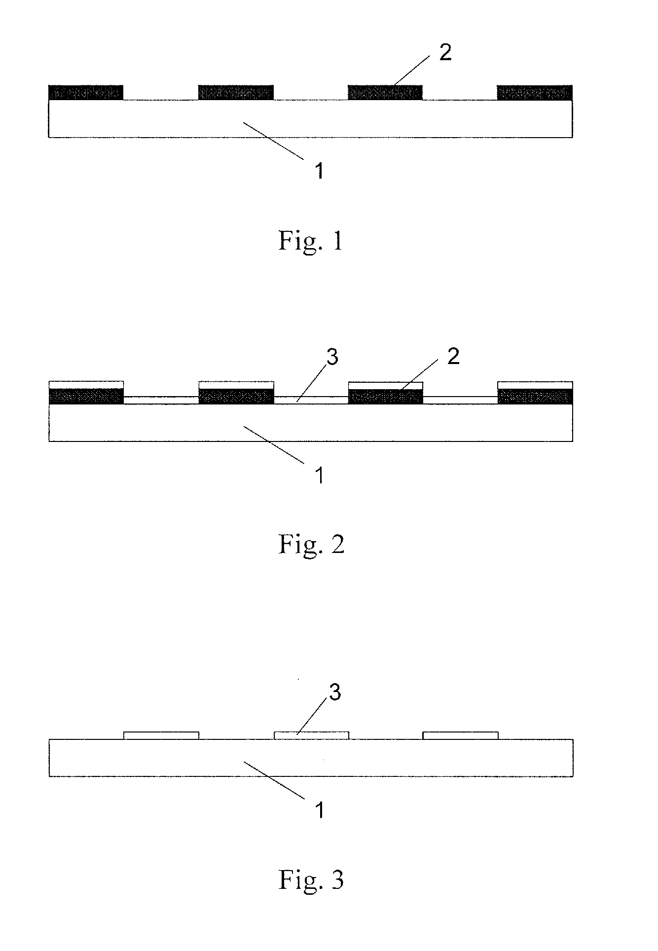
[0034]Step 1. a PMMA layer 2 with a thickness of 5 μm is coated on a glass substrate 1 by a spin-coating method, and then patterned by using electron beam. In this step, the PMMA layer in a region for forming the patterned graphene film is removed, as shown in FIG. 1.
[0035]Step 2. a solution of oxidized graphene is prepared.
[0036]For example, the solution of oxidized graphene is prepared as follows: under a condition of ice water bath, mixing 1 g graphite, 0.25 g sodium nitrate and 11.75 ml concentrated sulfuric acid (98%) in a 200 ml beaker and stirring; slowly adding 1.5 g potassium permanganate; stirring under 35° C. until the resultant solution becomes paste-like; quickly adding 46 ml de-ionized water and stirring for 15 minutes; adding 140 ml de-ionized water and 1.5 ml aqueous hydrogen peroxide solution and stirring for 10 minutes; filtering the resultant suspending so...
example 2
[0040]In the Example 2, the method of manufacturing the patterned graphene film comprises the following steps.
[0041]Step 1. a positive photoresist layer 2 with a thickness of 10 μm is coated on a substrate 1 formed of PET (polyethylene terephthalate) film by a spin-coating method, and then patterned by using ultraviolet. In this step, the photoresist layer in a region for forming the patterned graphene film is removed, as shown in FIG. 1.
[0042]Step 2. a solution of oxidized graphene is prepared.
[0043]For example, the solution of oxidized graphene is prepared as follows: under a condition of ice water bath, mixing 1.5 g graphite, 0.35 g sodium nitrate and 11.75 ml concentrated sulfuric acid (98%) in a 200 ml beaker and stirring; slowly adding 2.0 g potassium permanganate; stirring under 40° C. until the resultant solution becomes paste-like; quickly adding 46 ml de-ionized water and stirring for 15 minutes; adding 140 ml de-ionized water and 1.5 ml aqueous hydrogen peroxide solution ...
example 3
[0047]In the Example 3, the method of manufacturing the patterned graphene film comprises the following steps.
[0048]Step 1. a negative photoresist layer 2 with a thickness of 1 μm is coated on a substrate 1 formed of Al foil by a spin-coating method, and then patterned by using ultraviolet. In this step, the photoresist layer in a region for forming the patterned graphene film is removed, as shown in FIG. 1.
[0049]Step 2. a solution of oxidized graphene is prepared.
[0050]For example, the solution of oxidized graphene is prepared as follows: under a condition of ice water bath, mixing 0.5 g graphite, 0.20 g sodium nitrate and 10.75 ml concentrated sulfuric acid (98%) in a 200 ml beaker and stirring; slowly adding 1.2 g potassium permanganate; stirring under 25° C. until the resultant solution becomes paste-like; quickly adding 46 ml de-ionized water and stirring for 30 minutes; adding 140 ml de-ionized water and 1.5 ml aqueous hydrogen peroxide solution and stirring for 30 minutes; fi...
PUM
| Property | Measurement | Unit |
|---|---|---|
| Temperature | aaaaa | aaaaa |
| Temperature | aaaaa | aaaaa |
| Temperature | aaaaa | aaaaa |
Abstract
Description
Claims
Application Information
 - R&D
- Intellectual Property
- Life Sciences
- Materials
- Tech Scout
- Unparalleled Data Quality
- Higher Quality Content
- 60% Fewer Hallucinations
Browse by: Latest US Patents, China's latest patents, Technical Efficacy Thesaurus, Application Domain, Technology Topic, Popular Technical Reports.
© 2025 PatSnap. All rights reserved.Legal|Privacy policy|Modern Slavery Act Transparency Statement|Sitemap|About US| Contact US: help@patsnap.com