
Build-up printed circuit board and method of manufacturing the same

a technology of printed circuit boards and build-up, which is applied in the direction of resistive material coating, metallic material coating process, synthetic resin layered products, etc., can solve the problems of increasing surface roughness, difficult to implement fine circuits, and limited space for storing wire substrates constituting electric circuits with a variety of small-size and thin electronic devices

Inactive Publication Date: 2013-05-30
SAMSUNG ELECTRO MECHANICS CO LTD
View PDF0 Cites 6 Cited by
  • Summary
  • Abstract
  • Description
  • Claims
  • Application Information

AI Technical Summary

Benefits of technology

The present invention is about a way to make a printed circuit board that is reliable and has tiny circuits. The invention improves the bonding between a layer of resin and a layer of metal, which means there will be more reliable connections in the circuit board.

Problems solved by technology

However, a space for storing a wire substrate constituting an electric circuit accompanying with a variety of small-size and thin electronic devices is quite limited.
A conventional SAP forms a metal seed layer through a wet process to which wet surface processing and electropless plating are applied, which increases surface roughness, making it difficult to implement the fine circuit, and produces a large amount of wastes, being environment-unfriendly.

Method used


Image

  • Build-up printed circuit board and method of manufacturing the same
  • Build-up printed circuit board and method of manufacturing the same
  • Build-up printed circuit board and method of manufacturing the same

Examples


preparation example 1

[0061]Preparation of Epoxy Emulsion

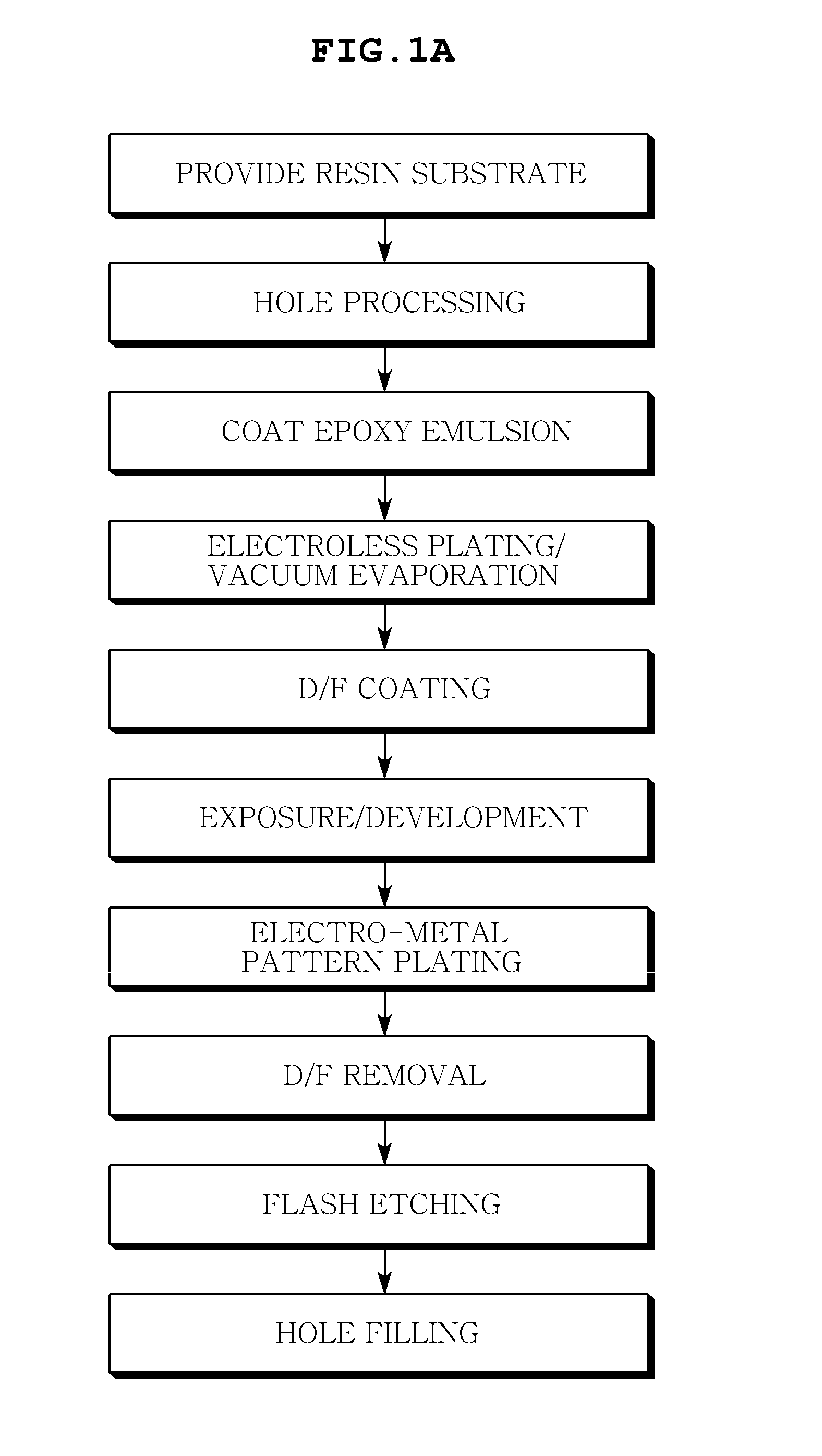
[0062]Epoxy resin (YDCN-500-90P) of 300 g and a surfactant (SDBS) of 60 g were melt in a dry oven for one hour at a temperature of about 120° C., the melt solution was cooled at a temperature of 70˜80°C., and a curing agent AEP of 10 wt % with respect to an epoxy weight was mixed with the solution. Then, a solid content of about 25 wt % was added to de-ionize water of 50° C. or higher to produce reverse emulsion, and a high speed homogenizer was forcibly mixed at an agitating speed of 12,000 rpm, and thus epoxy emulsion was prepared.

example 1

[0063]A. A via hole of about 100˜300 μm was formed in an epoxy resin substrate by using a computer numerical control (CNC) drill that is a mechanical drill, the prepared epoxy emulsion was coated on the epoxy resin substrate by using spray, and a surface roughness of the epoxy resin substrate was formed. Then, a Cu seed layer was deposited on the epoxy resin substrate in which the via hole was formed by using electroless plating. Thereafter, a pattern copper plating layer of about 10˜20 μm was formed through electro copper pattern plating at H2SO4 (120˜160 gl / l), Cu (20˜40 g / l), Cl (20˜50 ppm), Cupracid HL leveler (5-15 ml / l), air flow volume (0.05˜0.15 m3 / min), a temperature (20˜25° C.), and a current density (F / B1.5ASD), and the Cu seed layer was removed by performing flash etching by using a H2SO4 / H2O2 etching solution at an etching speed of 2 m / min. Finally, a core circuit layer was completely formed by filing the via hole at conditions of a copper paste having a viscosity of 3....

example 2

[0067]A CBGA substrate was manufactured in the same manner as described in Example 1 except that an ion beam sputter was used instead of using the electroless plating method during the process A of Example 1.

[0068]Results obtained by measuring a bonding intensity of a build-up PCB and a surface roughness of an insulation material thereof are shown in Table 1 below.


PUM

PropertyMeasurementUnit
Temperatureaaaaaaaaaa
Thicknessaaaaaaaaaa
Sizeaaaaaaaaaa

Abstract

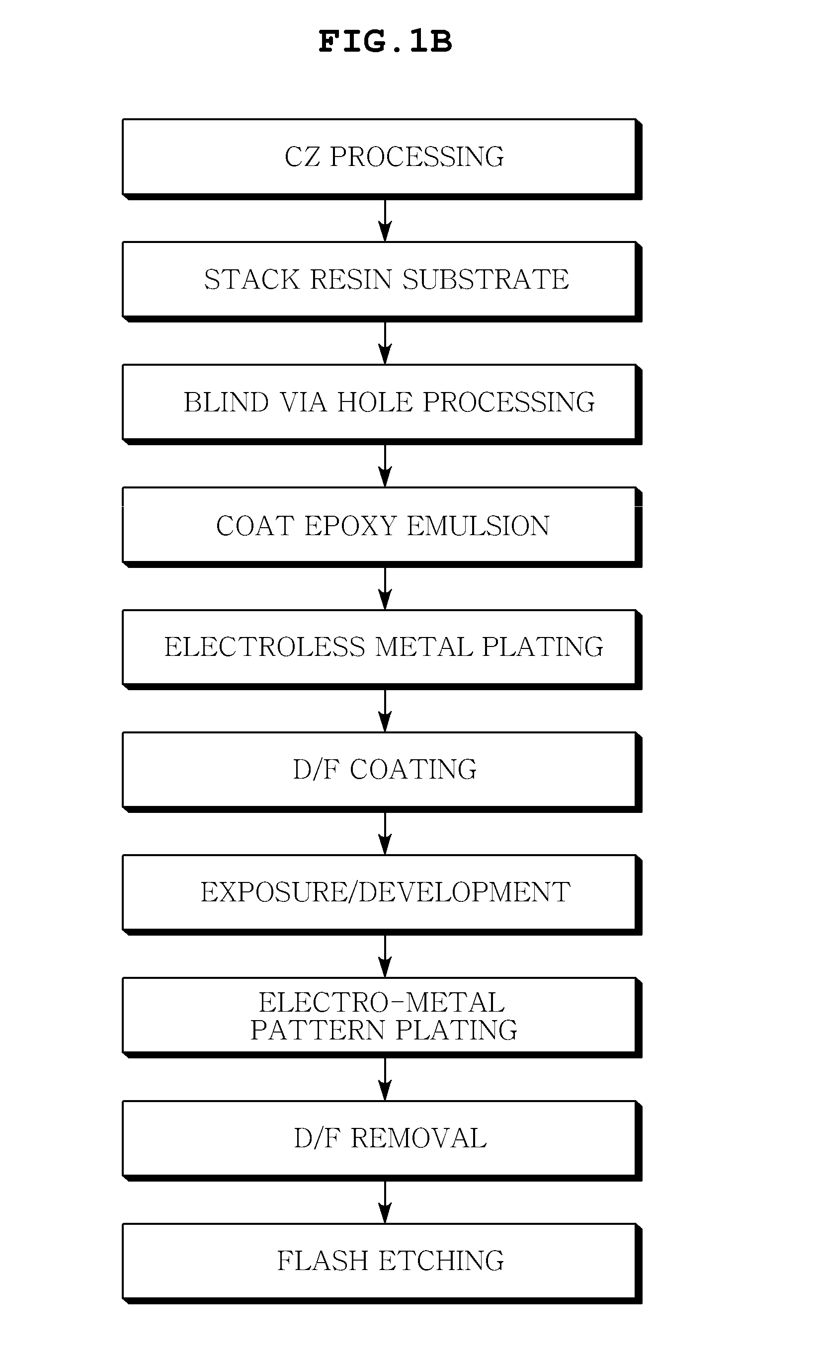
Disclosed herein is a method of manufacturing a build-up printed circuit board (PCB), the method including: providing a first resin substrate; forming a roughness by coating an epoxy emulsion solution on a surface of the first resin substrate; and providing a core layer by forming a core circuit layer on the first resin substrate on which the roughness is formed. According to the present invention, roughness of a substrate can be formed in an environment-friendly and economical way by introducing a process of coating epoxy emulsion on a resin substrate. Further, a highly reliable fine circuit can be implemented by enhancing an adhesive bond between a build-up board material and a metal circuit layer.

Description

CROSS REFERENCE TO RELATED APPLICATION[0001]This application claims the benefit of Korean Patent Application No. 10-2011-0124491, filed on Nov. 25, 2011, entitled “Build-up Printed Circuit Board and Producing Method Thereof”, which is hereby incorporated by reference in its entirety into this application.BACKGROUND OF THE INVENTION[0002]1. Technical Field[0003]The present invention relates to a build-up printed circuit board and a method of manufacturing the same.[0004]2. Description of the Related Art[0005]A high density print board is required to accompany a high function electronic device and a high integration semiconductor device, and a current mainstream thereof is a multilayer board. A stacked bonding method and a build-up method are known as methods of manufacturing a multilayer printed circuit board (PCB).[0006]The stacked bonding method, as disclosed in, for example, Japanese Patent Laid-Open Publication No. 62-205690, stacks a plurality of insulation substrates in which a...

Claims


Application Information

Patent Timeline
IPC IPC(8): H05K1/00H05K3/46C25D5/02H05K3/00
CPCH05K3/381H05K3/4602H05K3/4673H05K2201/0195C23C18/2066C25D3/38C25D5/026C25D5/56C23C18/1653H05K2203/1366H05K3/46H05K3/18
Inventor KIMSEO, YOUNG KWANKIM, JUN YOUNGCHO, SUNG NAM
Owner SAMSUNG ELECTRO MECHANICS CO LTD
Learn More