
Low temperature contact structure for flexible solid state device

a solid-state device, low-temperature technology, applied in semiconductor devices, lighting and heating apparatus, instruments, etc., can solve the problems of long manufacturing time, shorten the useful life of the device, and difficult to provide a reliable electrical connection, so as to achieve convenient and reliable electrical connection, maintain flexibility, and simplify manufacturing

Inactive Publication Date: 2012-10-11
GENERAL ELECTRIC CO
View PDF8 Cites 10 Cited by
  • Summary
  • Abstract
  • Description
  • Claims
  • Application Information

AI Technical Summary

Benefits of technology

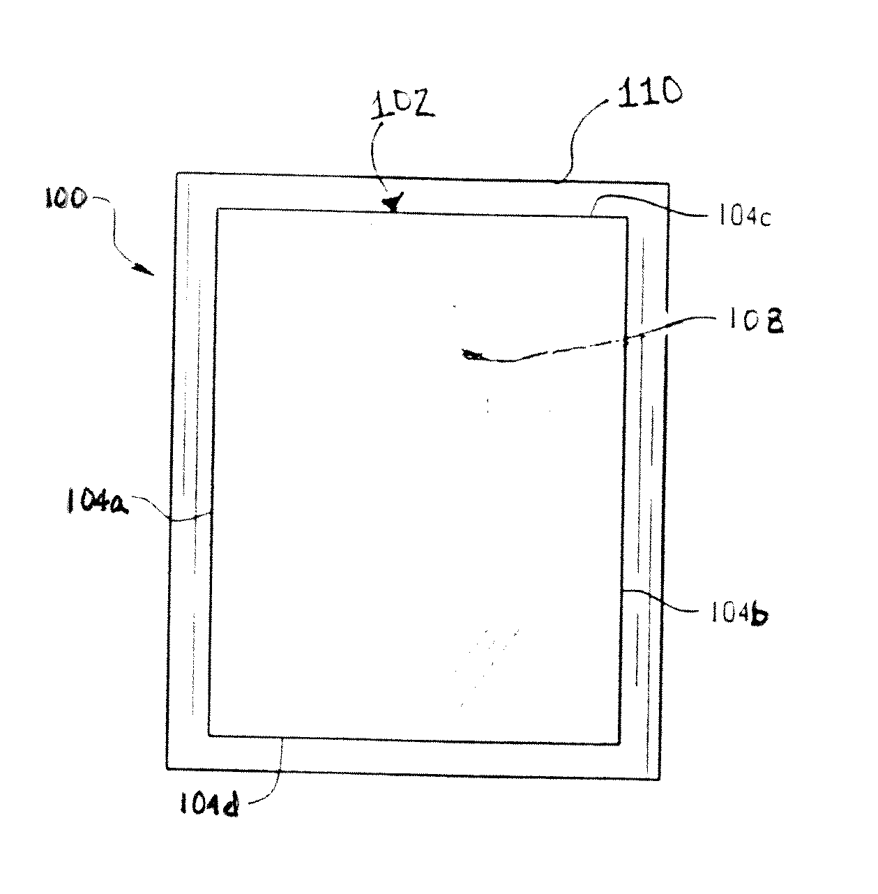
[0012]The backsheet includes a metallic patch that covers the feed-through region, providing an electrical pathway to the light source while maintaining the hermetic nature of the panel. This patch material in the area of the feed-through region(s) must also maintain the flexible nature of the device while providing a surface for a reliable and durable electrical connection. This material, which may for example be silver, copper, tin, nickel, gold or a combination thereof, must be compatible with the adhesive material within the hermetic package to prevent delamination and consequent failure due to oxygen and water vapor ingress, and it must also have properties that make it amenable to low temperature soldering techniques, i.e., it must have a high bond strength to the low temperature solder, exhibit low interface resistance, and have good oxidation resistance. The acceptable patch material must, therefore, be impermeable to oxygen and water vapor (e.g. having substantially no pin hole defects), provide good adhesion to the backsheet, be flexible, and in addition be burr-free to prevent possible shorting of the electrical device, which could occur if the patch edge(s) contact the inner metal foil in the backsheet through punctures in the outer layer.
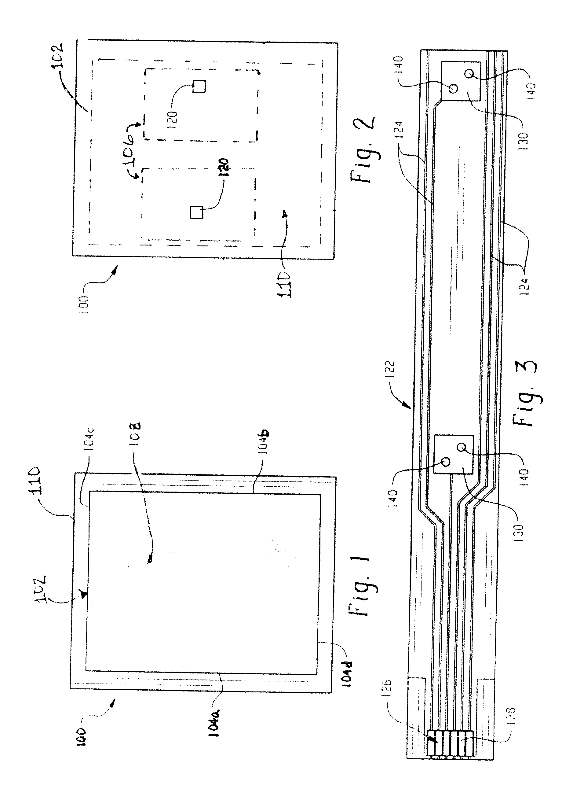
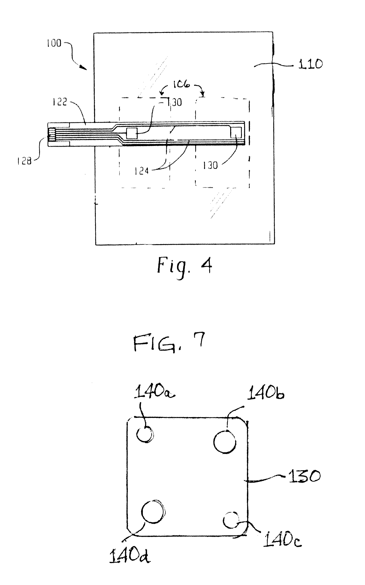
[0014]An associated method of assembling a light panel includes providing a substantially planar light source having a light emitting surface, a backsheet extending in substantially parallel relation therewith, and at least one electrical feed-through region in the backsheet located inwardly from a periphery of the substantially planar light source. Positioned over the electrical feed-through region is a flexible patch allowing an electrical pathway to the light panel as well as maintaining the hermetic seal of the entire device to prevent degradation from water and / or oxygen. Positioning a connector cable over the backsheet, including the patch, is a part of the assembly method so that a first portion of the connector cable extends outwardly of the light source periphery for connection with an associated drive circuit. The method further includes electrically connecting a second portion of the connector cable with the electrical feed-through region of the backsheet through the patch. The electrical connection is established between the connector cable and the patch using a low temperature solder composition that resists delamination, is oxidation resistant, and maintains the flexibility of the light panel.
[0021]A primary benefit is the ability to provide an effective, reliable electrical pathway for the panel from a region external of the panel while maintaining flexibility. Yet another benefit is found in the thin profile maintained by the lighting assembly when using a flat flex connector cable, along with the flexibility of the low temperature solder and, if used, the insulator sheet that allow for conformable lighting solutions.
[0022]Openings in the conductive pad of the flat flex cable simplify manufacturing, allowing the flat flex cable to be initially positioned, and then a bonding material applied to insure positional accuracy.
[0024]In addition to the foregoing, this method provides an option to construct a lighting assembly in a single lamination process, thus providing a more economical assembly, as well as providing for ease in uniformly illuminating a large area, interconnecting multiple devices, and maintaining flexibility of the panel.
[0025]Still further, the use of a low temperature solder as disclosed herein for electrically connecting the patch and the connector cable allows for efficient, fast processing at lower temperatures, in keeping with the temperature sensitive processing limits of the OLED, as compared to other known epoxy or tape adhesive arrangements and materials.

Problems solved by technology

Preferably, the panel is hermetically sealed since moisture and oxygen have an adverse impact on the OLED device.
The flexible nature of the OLED and the temperature tolerance level of the OLED panel combine to make providing a reliable electrical connection difficult.
While it is known to use silver epoxy or double-sided conductive tape in the area of the connection, both suffer from problems due to early delamination and poor electrical properties, thus shortening the useful life of the device.
This long manufacturing time is the result of the higher temperatures needed in order to render an acceptable connection, which is limited by the temperature parameters of the OLED, which are much lower than the higher temperatures at which such materials are generally processed.
Therefore, it takes a longer period of time at a lower temperature to render a connection that is acceptable, but not necessarily up to the desired standard.

Method used


Image

  • Low temperature contact structure for flexible solid state device
  • Low temperature contact structure for flexible solid state device
  • Low temperature contact structure for flexible solid state device

Examples


example 1

Low Temperature Solder Process

[0052]This Example may be understood best with reference to FIG. 10 providing an exploded view of one embodiment of a finished device in accord herewith. In particular, this process demonstrates the use of low temperature solder 160 to connect a flat flex cable 122 to patch 106 of lighting assembly 100. In this example, two different low temperature solder compositions were obtained from Indium Corporation. The first was an alloy of In(51)-Bi(32.5)-Sn(16.5), having a liquidus temperature (melting point) of 61° C., and the second was an alloy having the composition Bi(57)-In(26)-Sn(17), with a liquidus temperature of 79° C. The patch material comprised hot tin dipped copper, available commercially from All Foils, Inc., cut to 30 mm×60 mm dimensions and rendered burr-free. The flat flex cable included tin coated copper connection pads, generally in accord with that shown in FIG. 5. Other materials included flux, commercially available from Indium Corporat...


PUM


Abstract

A lighting assembly includes a light source having a first generally planar, light source including a perimeter edge. A backsheet is disposed in substantially parallel relation with the light source, and includes at least one electrical feedthrough region extending through the backsheet and substantially covered by a contact patch disposed in substantially planar relation between the backsheet and the light source. A generally planar, connector cable extends over the backsheet and has connector pad(s) positioned thereon to associate with each feedthrough and to the light source through the contact patch. A low temperature solder material is disposed between each connector pad and contact patch for establishing electrical connection with the light source, wherein one or more of the light source, connector cable, backsheet, or any portion thereof is constructed of one or more plastics.

Description

BACKGROUND OF THE DISCLOSURE[0001]The present disclosure relates to a light source and particularly a light source connection and a method for providing the same. More particularly, the disclosure relates to a light emitting device such as an organic light emitting diode panel and connection, as well as to low temperature materials and methods suitable for providing electrical connection to such a panel.[0002]Organic light emitting diode (OLED) devices are generally known in the art. An OLED device typically includes one or more organic light emitting layer(s) disposed between electrodes. For example, a cathode, organic layer, and a light-transmissive anode formed on a substrate emit light when current is applied across the cathode and anode. As a result of the electric current, electrons are injected into the organic layer from the cathode and holes may be injected into the organic layer from the anode. The electrons and holes generally travel through the organic layer until they r...

Claims


Application Information

Patent Timeline
IPC IPC(8): G09G3/32H05B44/00
CPCF21Y2105/008H01L51/5203H05K1/189H01L2251/5361H05K1/113H01L2251/5338F21Y2105/00F21Y2115/15H10K50/805H10K2102/311F21Y2105/14H10K71/70
Inventor KOSTKA, JAMES MICHAELAURONGZEB, DEEDERROBERTS, BRUCE RICHARDBRNADA, JOSIP
Owner GENERAL ELECTRIC CO
Learn More