Wiring board and method of manufacturing the same

Inactive Publication Date: 2012-06-21
NGK SPARK PLUG CO LTD
View PDF5 Cites 13 Cited by
  • Summary
  • Abstract
  • Description
  • Claims
  • Application Information

AI Technical Summary

Benefits of technology

[0042]The manufacturing method of a wiring board of the present invention allows for high-density packaging of conductor posts 16. That is, the wiring boards 10 may have conductor posts 16 having larger aspect ratios (ratio of height to width) than those in the related art. Accordingly, even for conductor posts 16 with small pitches, sufficient height from the surface of the solder resist layer can be attained. Furthermore, high connection reliability can be achieved between the wiring board 10 and a part to be packaged in this wiring board 10 by using a conductor post 16.
[0048]Embodiments of the wiring boards of the present invention are able to allow for high-density packaging of conductor posts 16. That is, the wiring boards 10 may include conductor posts 16 having larger aspect ratios (ratio of height to width) than those in the related art. According to this, even for conductor posts 16 having a small pitch, sufficient height from the surface of the solder resist layer can be attained. Furthermore, connection with high reliability can be achieved between the wiring board 10 and a part to be packaged in this wiring board 10 by using such a conductor post 16. Further, since the solder resist layer 13 may include a thermosetting resin and the first conductor part 181 composed mainly of copper, the thermal expansion coefficient of the solder resist layer 13 and the first conductor part 181 decreases, and therefore a durability of the entire wiring board against stress at the time of mounting a semiconductor chip, such as IC chip, on the wiring board can be improved.

Problems solved by technology

The formation of bumps having high aspect ratios required for the foregoing high-density packaging is relatively difficult.
However, in the case where a solder resist layer 13 is thick, or the diameter of a through-hole 131 formed in the solder resist layer 13 is small, the fabrication of the mask 22 per se is difficult, and it is also difficult to sufficiently ensure its precision.
Furthermore, even when a mask 22 can be formed, the diameter of the through-hole 131 opened in the mask 22 is small, which causes problems such as clogging within the mask 22 and the paste solder 30 being hardly printed.

Method used


Image

  • Wiring board and method of manufacturing the same
  • Wiring board and method of manufacturing the same
  • Wiring board and method of manufacturing the same

Examples


embodiment

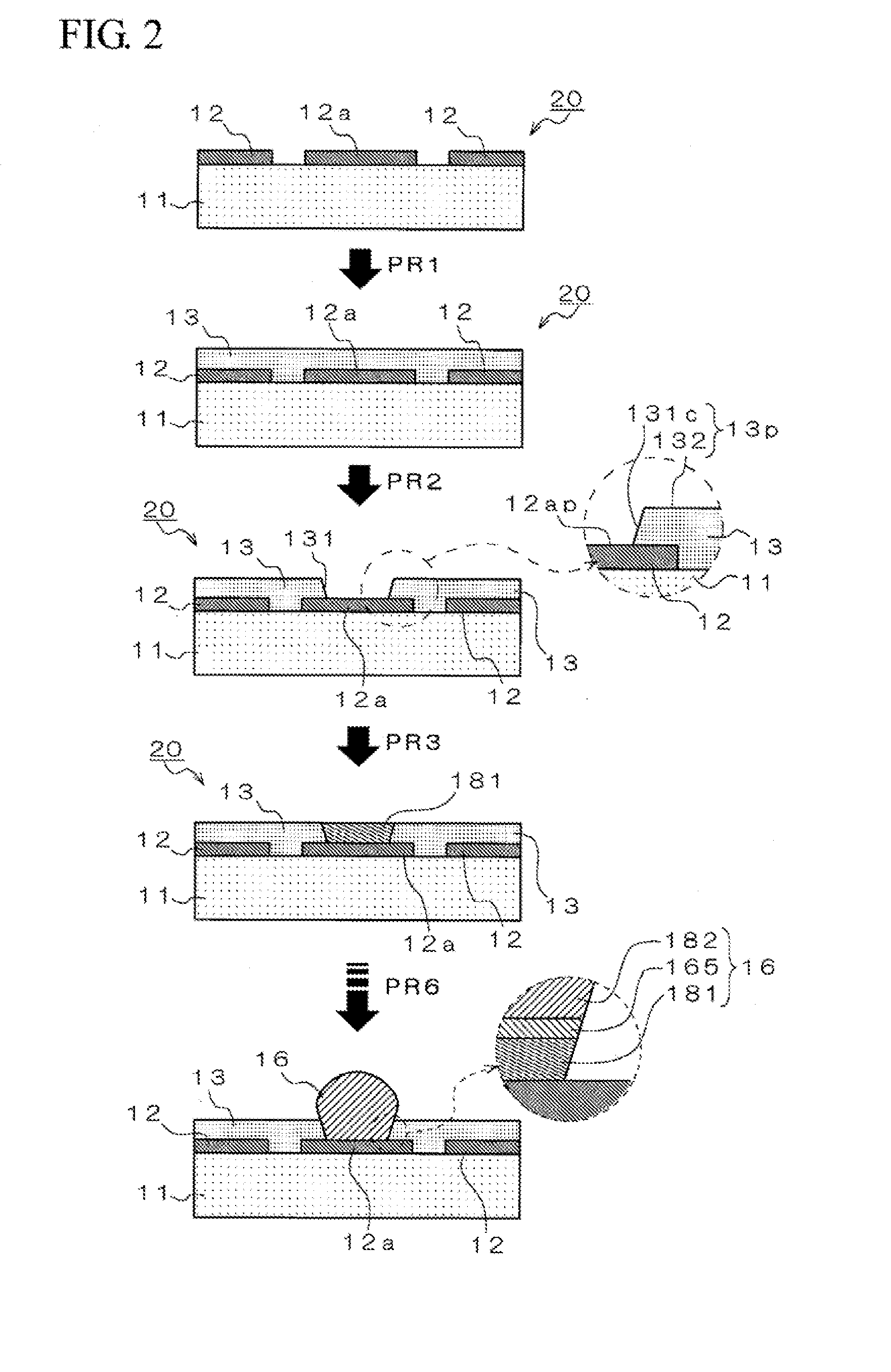
[0136]a wiring board 10 of the invention is more specifically described below with respect to the following Embodiment, but it should not be construed that the invention is limited to this Embodiment.

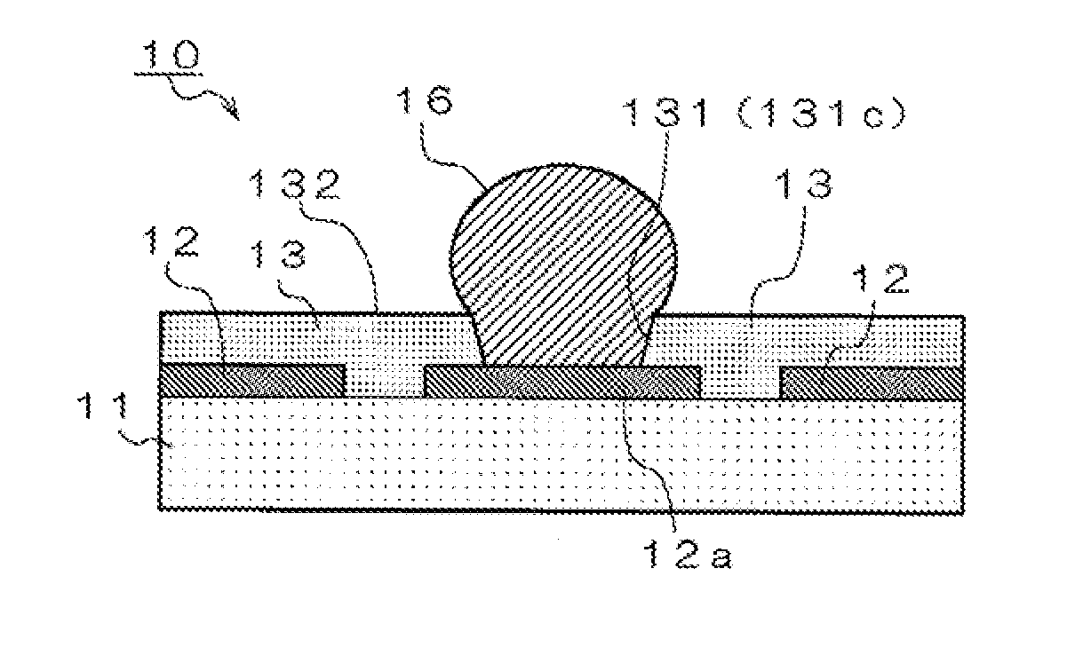
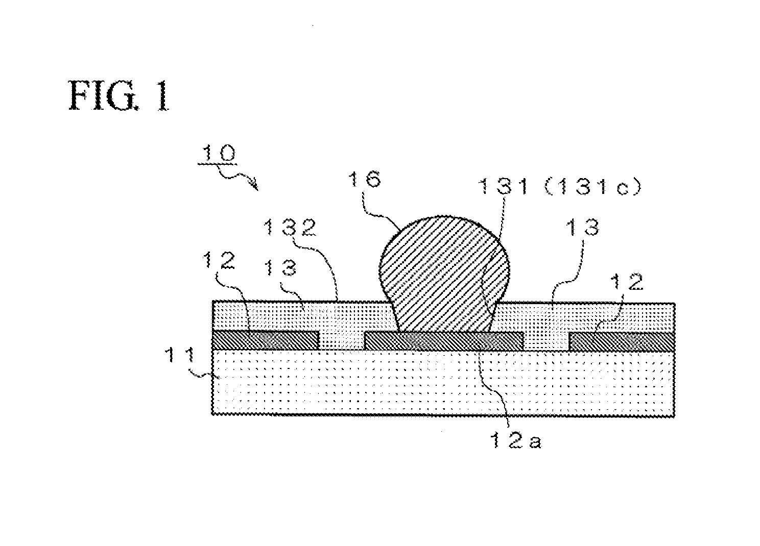
[0137](1) Wiring Board 10:

[0138]A wiring substrate 10 (see FIG. 1) manufactured according to this Embodiment includes a conductor layer 12 laminated on the side of one surface of a core substrate 11, a solder resist layer 13 laminated on this conductor layer 12, and a conductor post 16 to be electrically connected to a conductor layer 12a which is disposed in a lower portion of a through-hole 131 provided in the solder resist layer 13. The core substrate 11 is composed of glass epoxy (epoxy resin containing glass fibers as a core material) having a thickness of 0.8 mm. Also, the conductor layer 12 is one obtained by patterning a copper foil having a thickness of 12 μm on one surface of the core substrate 11. Furthermore, the solder resist layer 13 has a thickness of 21 μm and contains a...


PUM

PropertyMeasurementUnit
Electrical conductivityaaaaaaaaaa

Abstract

Disclosed is a method for manufacturing a wiring board including a conductor layer, a solder resist layer laminated on the conductor layer, and a conductor post to be electrically connected to a conductor layer which is disposed in a lower portion of a through-hole provided in the solder resist layer, the method including a through-hole boring process of boring the through-hole in the solder resist layer containing a thermosetting resin to expose the conductor layer within the through-hole; a first conductor part forming process of forming a first conductor part composed mainly of copper within the through-hole; and a second conductor part forming process of forming a second conductor part composed mainly of tin, copper, or a solder on the first conductor part, in this order.

Description

CROSS-REFERENCE TO RELATED APPLICATIONS[0001]The present application claims priority from Japanese Patent Application No. 2010-279707, which was filed on Dec. 15, 2010, and Japanese Patent Application No. 2011-227310, which was filed on Oct. 14, 2011, the disclosure of which is herein incorporated by reference in its entirety.BACKGROUND OF THE INVENTION[0002]1. Field of the Invention[0003]The present invention relates to a wiring board and a method of manufacturing the same. In more detail, embodiments of the present invention relate to wiring boards having a conductor post and methods of manufacturing such wiring boards.[0004]2. Description of Related Art[0005]In recent years, as a high-density packaging technique, for example, a C4 (controlled collapse chip connection) method has been adopted. Wiring boards utilized in C4 methods have a surface that is covered by a solder resist layer, and wherein a bump (conductor post) is vertically arranged, in an optionally bored opening in th...

Claims


Application Information

Patent Timeline
IPC IPC(8): H05K1/09B23K31/02B23K1/20H05K3/10
CPCB23K1/0016B23K2201/42H01L24/16H05K3/3473H05K3/3478H05K2203/1476H05K2201/0341H05K2203/041H05K2203/043H05K2203/054H05K2203/0574H01L2224/16225B23K2101/42H01L2924/14H01L2924/00H01L23/12H05K1/18H05K3/34
Inventor YAMADA, ERINAHIGO, KAZUNAGASATO, HIRONORI
Owner NGK SPARK PLUG CO LTD
Why Eureka
Try Eureka