
Photovoltaic cell

a photovoltaic cell and photovoltaic junction technology, applied in the field of photovoltaic junctions, can solve the problems of large loss of potential electrical power of shorter wavelength photons, limited devices, and low gainp

Inactive Publication Date: 2011-07-28
LUMENTUM OPERATIONS LLC
View PDF4 Cites 17 Cited by
  • Summary
  • Abstract
  • Description
  • Claims
  • Application Information

AI Technical Summary

Benefits of technology

[0012]The invention provides a photovoltaic junction having an intrinsic region comprising a series of quantum wells formed of an InGaAsP quaternary material. Such a compound enables the absorption edge obtained using a tertiary GaInP material to be extended to longer wavelengths.
[0013]It has been found that this quaternary material can be grown with good mixing of the group III atoms, to provide the high material quality which is critical in forming a quantum well photovoltaic junction for high efficiency operation. By suitable adjustment of the complementary In and Ga proportions and the complementary As and P proportions, the absorption edge of the material can be controlled over a significant range of wavelengths as may be desired, for example, to tune the performance of the junction when used in a tandem solar cell, while at the same time yielding a well material with a required lattice parameter. In this way, for example, materials described in detail below which are closely lattice matched to GaAs (or another substrate such as Ge) with a tunable band edge between about 700 nm and 800 nm in wavelength can easily be obtained, although a range of about 700 nm to 740 nm is particularly useful in some of the described applications. Similar materials which are not lattice matched to the substrate, but which are used in a stress balanced structure with compensating barrier structures can also be obtained.
[0018]The quantum wells are separated by barrier layers. Conveniently, these may be of tertiary GaInP material. The alternate barrier and well layers may then be grown using an epitaxial technique by turning the Arsenic source on and off. Because Arsenic atoms generally incorporate into the epitaxial growth much more easily than Phosphorous atoms, much less Arsenic feed material is required than Phosphorous feed material and only small changes in the amount of Arsenic feed material is required, hence the proportion of Arsenic incorporated can be controlled accurately and simply. The barriers may more generally be formed of a semiconductor material comprising Ga, In and P, including quaternary materials further incorporating, for example, Al, As, N or Sb.
[0021]Conveniently, however, the materials of the wells and barriers may be chosen such that the lattice constants of the well material and the barrier material both substantially match that of the substrate. This permits the thicknesses of the well and barrier layers to be chosen independently of stress balancing constraints. This can help allow a greater total thickness of quantum wells in the intrinsic region.
[0023]According to one variation, the InGaAsP wells may be grown as stepped wells, by incorporating a subwell of GaAs separated from the barrier layers (typically of GaInP) by the quaternary InGaAsP material. This inclusion of GaAs subwells, to form stepped wells of InGaAsP—GaAs—InGaAsP, can extend the band edge of the structure out to a wavelength of about 850 nm. The InGaAsP layers help to stabilize the transition from GaInP which is free of As, to GaAs, which is free of P.

Problems solved by technology

However, a longer wavelength absorption edge generally gives rise to a photocurrent generated at a lower junction voltage, so that much of the potential electrical power from shorter wavelength photons is lost from rapid thermalisation of liberated charge carriers, within the junction, to the band gap energy corresponding to the absorption edge.
The device is therefore limited by the junction generating the smallest photocurrent.
In this light, the use of a quantum barrier / well intrinsic region in the upper junction formed of GaInP presents some problems.
Furthermore, the requirements of the stress balance condition limit the choices of quantum well and barrier thicknesses which enable one to achieve a certain absorption edge.
In addition, successive barrier and well layers of GaInP based materials are difficult to grow as a perfect solution, and without unwanted ordering of the group III Gallium and Indium materials whereby the Gallium and Indium atoms tend to form single-species regions on adjacent (111) planes, rather than being well mixed within the crystal structure.

Method used


Image

  • Photovoltaic cell
  • Photovoltaic cell
  • Photovoltaic cell

Examples


first embodiment

[0046]Referring now to FIG. 3, the structure of a solar cell according to the invention is shown schematically. Not all layers are necessarily shown in the diagram. Broadly, the cell comprises a substrate 20 on which is formed a lower photovoltaic junction 22. A tunnel junction 24 is formed on top of the lower junction 22, and an upper photovoltaic junction 26 is formed on the tunnel junction 24. Structures overlying the upper photovoltaic junction may include a window layer 28, and electrodes 30 will typically be provided on the window layer and underneath the substrate. The solar cell is operated by providing illumination 32, typically concentrated solar illumination, at the top of the cell, and drawing the generated electrical power by connections to the electrodes 30. The upper photovoltaic junction absorbs incident photons having an energy higher than a band edge of the junction. Photons of lower energy pass through to the lower junction which has a lower energy band edge. Sinc...

second embodiment

[0049]The choice of other materials in the solar cell will depend on various factors and constraints, and a particular detailed example is given below in the Typically, the substrate may be of GaAs or Germanium, and the lower photovoltaic junction may be a GaAs based junction. In particular the lower junction may be a p-i-n junction and have bulk semiconductor regions formed of GaAs. The intrinsic region of the lower junction may itself contain quantum wells, for example to extend the band edge of the junction to longer wavelengths. These wells and surrounding barriers may be stress or strain balanced in ways discussed in the prior art and elsewhere in this document, for example to enable the band edge of the intrinsic region to be extended to longer wavelengths. This is may be important for the device to make better use of the available spectrum of incident light. There may be other photovoltaic junctions in the device, between, above or below the lower and upper junctions, and / or...


PUM


Abstract

The disclosure relates to multiple quantum well (MQW) structures for intrinsic regions of monolithic photovoltaic junctions within solar cells which are substantially lattice matched to GaAs or Ge. The disclosed MQW structures incorporate quantum wells formed of quaternary InGaAsP, between barriers of InGaP.

Description

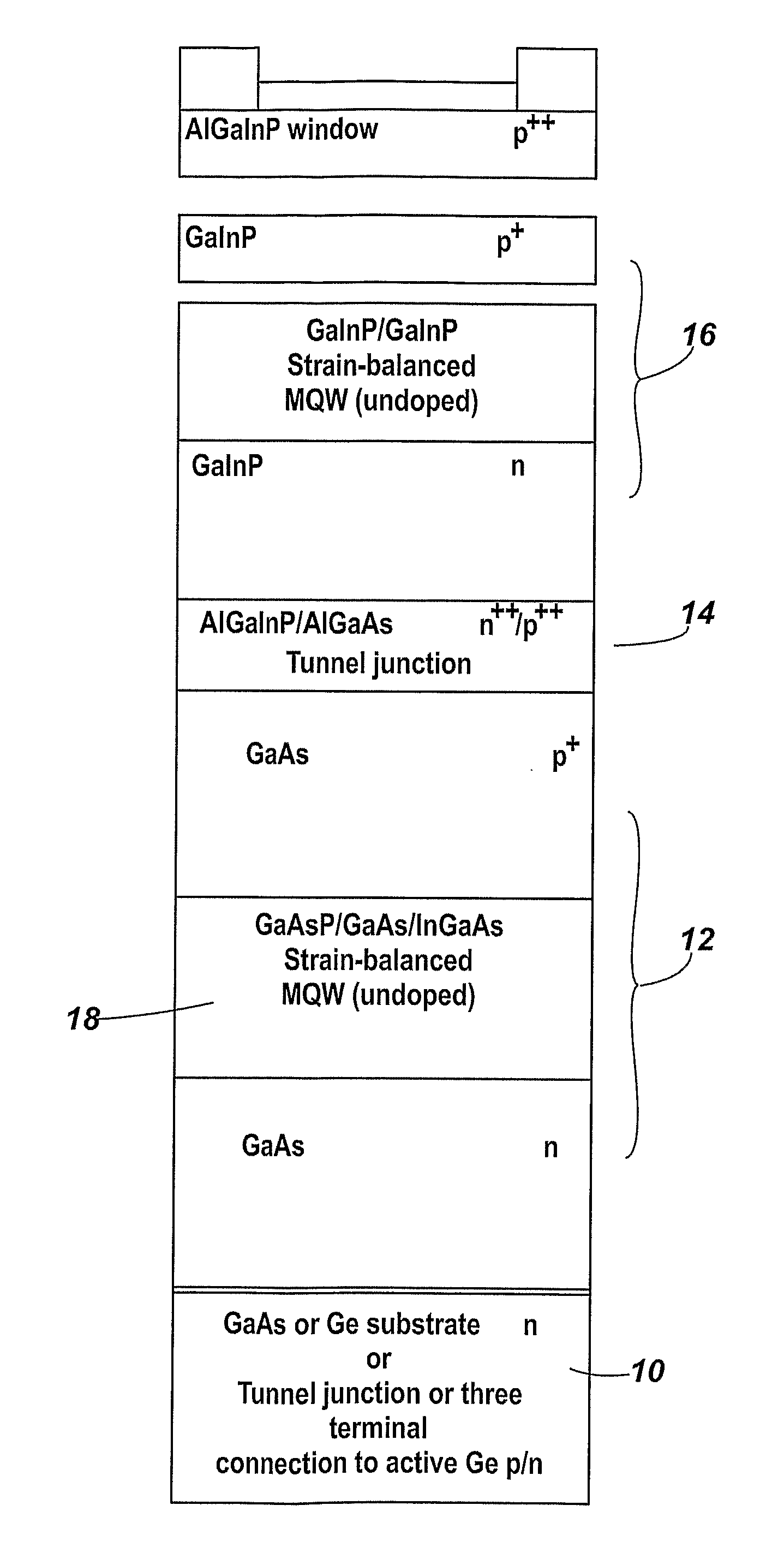
FIELD OF THE INVENTION[0001]The present invention relates to a photovoltaic junction having multiple quantum wells in an intrinsic region, and a photovoltaic cell comprising such a junction for generating electrical power from incident light, such as sunlight. In particular, but not exclusively, the junction may be used as the top junction in a tandem multiple junction solar cell adapted to receive highly concentrated sunlight, and having a lower photovoltaic junction based on GaAs having an absorption edge extended to longer wavelength by using multiple stress balanced quantum wells / barriers in an intrinsic region.Introduction[0002]US2005 / 0247339 describes a tandem solar cell illustrated in FIG. 7 of that document, and reproduced here as FIG. 1. The illustrated solar cell comprises a GaAs substrate 10 (with an active or passive Ge substrate as an alternative), a lower photovoltaic junction 12 grown on the substrate and adapted to generate electrical power from photons of wavelength...

Claims


Application Information

Patent Timeline
IPC IPC(8): H01L31/06H01L31/0352H01L31/076
CPCB82Y20/00H01L31/03046Y02E10/548H01L31/076Y02E10/544H01L31/035236H01L31/075
Inventor ROBERTS, JOHN
Owner LUMENTUM OPERATIONS LLC
Learn More