Surface-treated ceramic member, method for producing the same and vacuum processing apparatus
a technology of ceramic parts and surface treatment, applied in the direction of silicon oxides, transportation and packaging, liquid/solution decomposition chemical coatings, etc., can solve the problems of shortening the operation life of equipment, affecting the quality of the device, and unable to prevent particles completely, etc., to achieve excellent corrosion resistance
- Summary
- Abstract
- Description
- Claims
- Application Information
AI Technical Summary
Benefits of technology
Problems solved by technology
Method used
Image
Examples
example 1
[0058]Different ceramic bodies (surface roughness Ra: 0.7±0.1 μm, dimension: 30 mm×30 mm×2.5 mm) having the compositions and the porosities listed in Table 1 were prepared, and to these ceramic bodies, the coating film materials shown in Table 1 were applied and wiped off with waste cloth to prepare specimens. For each of the specimens, the area ratio of the coating film and the amount of the generated particles were obtained. For some Examples, the vacuum chamber components of semiconductor production equipment were actually fabricated, mounted in the apparatus and examined with respect to the use condition.
[0059]
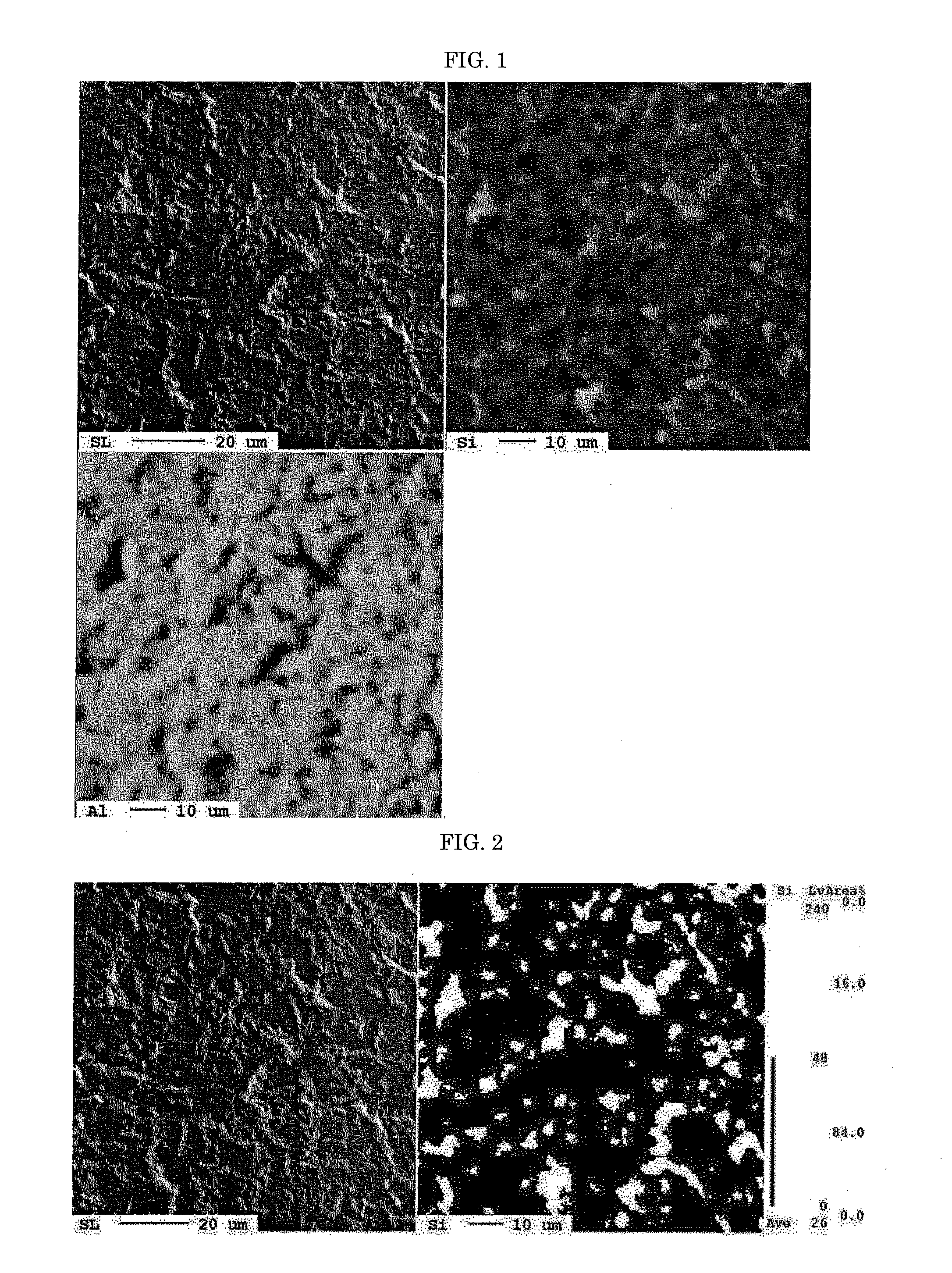
[0060]Each of the specimens was beforehand subjected to gold evaporation with a sputtering film formation apparatus for SEM test (SC-704, manufactured by Sanyu Electron Co., Ltd.) to form a conductive film, and a SEM image and the distributions of the elements derived from the ceramic body and the coating film material were scanned and mapped with an analyzer (JXA-8100, ma...
example 2
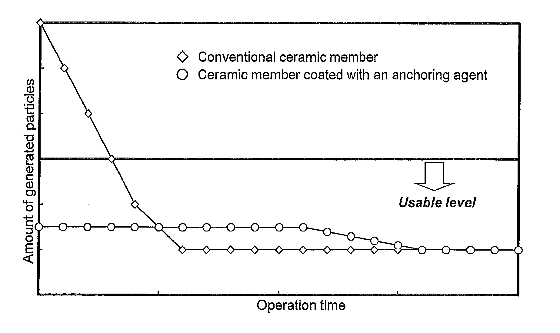
[0069]In each of Example Embodiment 3 of the present invention and Comparative Example 1 shown in Table 1, a ceramic member was disposed as a deposition preventive shield used in a plasma treatment chamber of semiconductor production equipment, and the number of generated particles was examined with a particle counter (SPI manufactured by KLA-Tencor Corp.). The examination was performed as follows: 25 wafers were plasma treated, and six wafers in total, namely, the first, fifth, tenth, 15th, 20th and 25th wafers were subjected to the measurement of the number of the particles of 1 μm or more present on the wafer. The results are shown in Table 2. The same ceramic member of Example Embodiment 3 of the present invention was subjected to five times of cleaning usually required for maintenance, then mounted again in a working apparatus, and then subjected to the examination of the number of generated particles in the same manner as described above. The result is also shown in Table 2 un...
PUM
| Property | Measurement | Unit |
|---|---|---|
| porosity | aaaaa | aaaaa |
| density | aaaaa | aaaaa |
| density | aaaaa | aaaaa |
Abstract
Description
Claims
Application Information
 - R&D
- Intellectual Property
- Life Sciences
- Materials
- Tech Scout
- Unparalleled Data Quality
- Higher Quality Content
- 60% Fewer Hallucinations
Browse by: Latest US Patents, China's latest patents, Technical Efficacy Thesaurus, Application Domain, Technology Topic, Popular Technical Reports.
© 2025 PatSnap. All rights reserved.Legal|Privacy policy|Modern Slavery Act Transparency Statement|Sitemap|About US| Contact US: help@patsnap.com


