
Nitride semiconductor layer-containing structure, nitride semiconductor layer-containing composite substrate and production methods of these

Inactive Publication Date: 2011-02-24
CANON KK
View PDF15 Cites 15 Cited by
  • Summary
  • Abstract
  • Description
  • Claims
  • Application Information

AI Technical Summary

Benefits of technology

[0054]Additionally, there can be realized the production method of the nitride semiconductor layer-containing structure that enables the base substrate removal in which the damage exerted on the nitride semiconductor layer is reduced.

Problems solved by technology

However, there has hitherto been a problem that it is difficult to produce high-quality nitride semiconductor films or high-quality nitride semiconductor substrates.
(1) The production process of the nitride semiconductor substrate involves high-cost steps.
For example, in the production of a GaN substrate, a high temperature and a high pressure are required, and it is difficult to produce a substrate low in defect density and large in caliber.
Accordingly, GaN substrates are high in price, and the stationary supply of GaN substrates to meet mass production is not available.
(2) The heterogeneous substrates suitable for the epitaxial growth of the high-quality nitride semiconductor films are scarce.
The heterogeneous single crystal substrates capable of withstanding such harsh conditions are limited.
(3) Depending on the devices, complicated structures are required due to the crystal properties of the nitride semiconductor itself.
Accordingly, when a heterogeneous substrate such as a sapphire substrate is used, there occurs a problem caused by the dislocation propagating in the nitride semiconductor film due to the lattice constant difference between the nitride semiconductor film and the heterogeneous substrate.
Additionally, there is also a problem that a stress strain occurs in the nitride semiconductor film and the heterogeneous substrate due to the difference of coefficient of thermal expansion between the nitride semiconductor film and the heterogeneous substrate.
On the other hand, also in the removal of the base substrate of the nitride semiconductor, there have hitherto been the problems typified by the long operation time and the damage exerted on the nitride semiconductor.
These problems are particularly remarkable when sapphire, which is hard, is used for the base substrate.
Accordingly, this technique offers a problem that in the crystal growth process of the nitride semiconductor film which requires a growth temperature of about 1000° C., the mask material is degraded to adversely affect the nitride semiconductor film.
For example, in the case where the mask material is SiO2, the components thereof, Si or O2, and in the case where the mask material is a Mg compound, the components thereof, Mg and others, diffuse into the nitride semiconductor film to adversely affect the quality or the carrier control of the nitride semiconductor film, as the case may be.
However, just a single layer of the void structure formed between the nitride semiconductor film and the substrate by the use of the asperity pattern provides an insufficient reduction of the threading dislocation and an insufficient alleviation of the stress strain.
Just with such a technique, it is not easy to form two or more layers of voids in intended shapes.
On the other hand, the technique disclosed in U.S. Pat. No. 6,979,584 enables to form two or more layers of voids, but offers a difficulty in ensuring the void size because both of the longitudinal growth and the lateral growth are effected at the same time.
Consequently, the effect due to the voids on the alleviation of the stress strain is low.
Consequently, the technique disclosed in Japanese Patent Application Laid-Open No. 2001-176813 by itself hardly avoids the damage exerted on the nitride semiconductor at the time of the removal of the base substrate.

Method used


Image

  • Nitride semiconductor layer-containing structure, nitride semiconductor layer-containing composite substrate and production methods of these
  • Nitride semiconductor layer-containing structure, nitride semiconductor layer-containing composite substrate and production methods of these
  • Nitride semiconductor layer-containing structure, nitride semiconductor layer-containing composite substrate and production methods of these

Examples


first embodiment

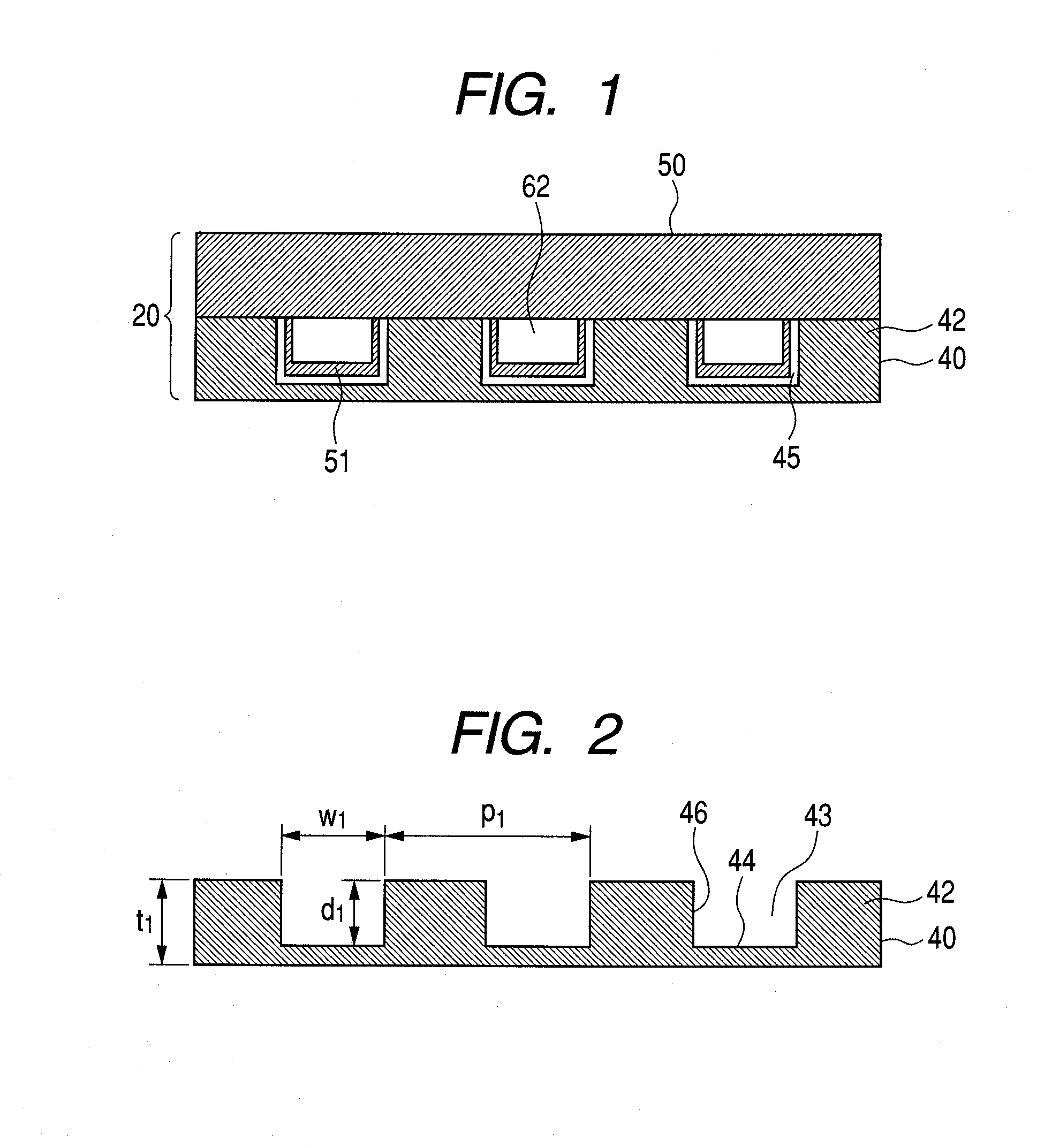
[0099]As a first embodiment of the present invention, an example of the nitride semiconductor-containing structure is described. FIG. 1 shows a schematic sectional view for illustrating an example of the nitride semiconductor-containing structure in the present embodiment.

[0100]FIG. 1 illustrates a nitride semiconductor-containing structure 20, a first nitride semiconductor layer 40, a raised portion 42 of the first nitride semiconductor layer and a crystallinity defect-containing portion 45 in the first nitride semiconductor layer.

[0101]FIG. 1 also illustrates a second nitride semiconductor layer 50, a nitride semiconductor 51 formed in a recessed portion of the first nitride semiconductor layer and a void 62 in the nitride semiconductor structure.

[0102]The nitride semiconductor-containing structure 20 of the present embodiment is formed of the first nitride semiconductor layer 40, the second nitride semiconductor layer 50, and the voids 62 in the nitride semiconductor structure fo...

second embodiment

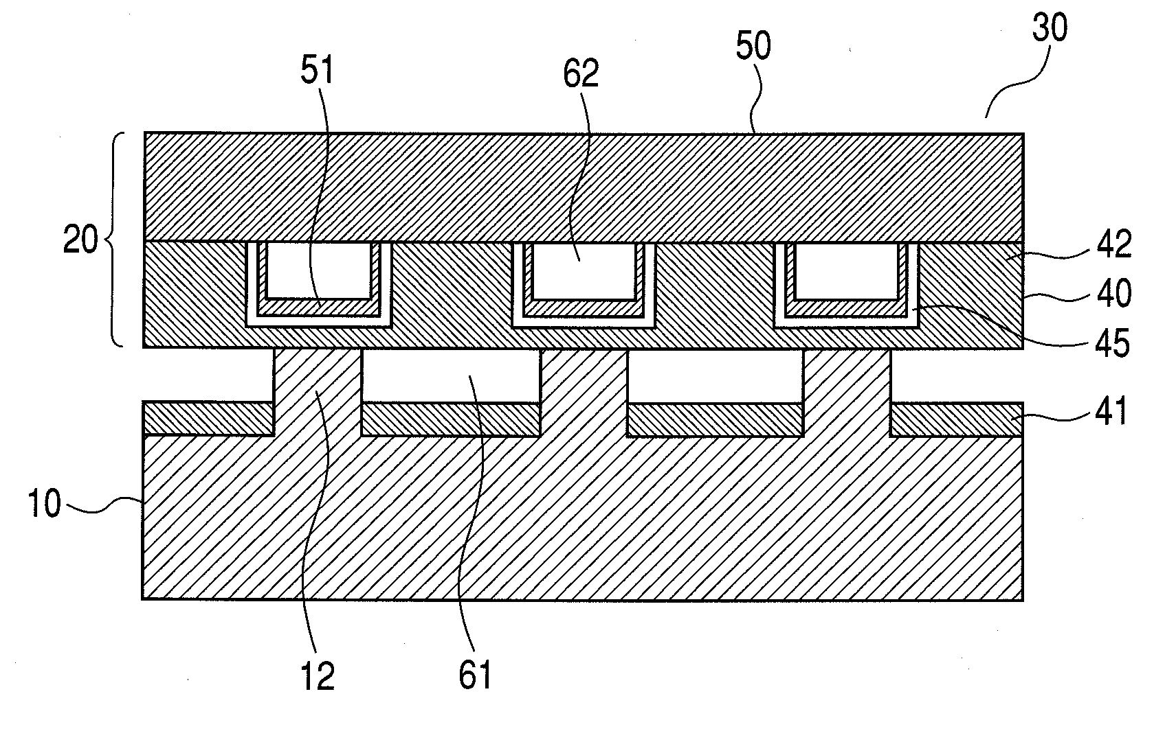
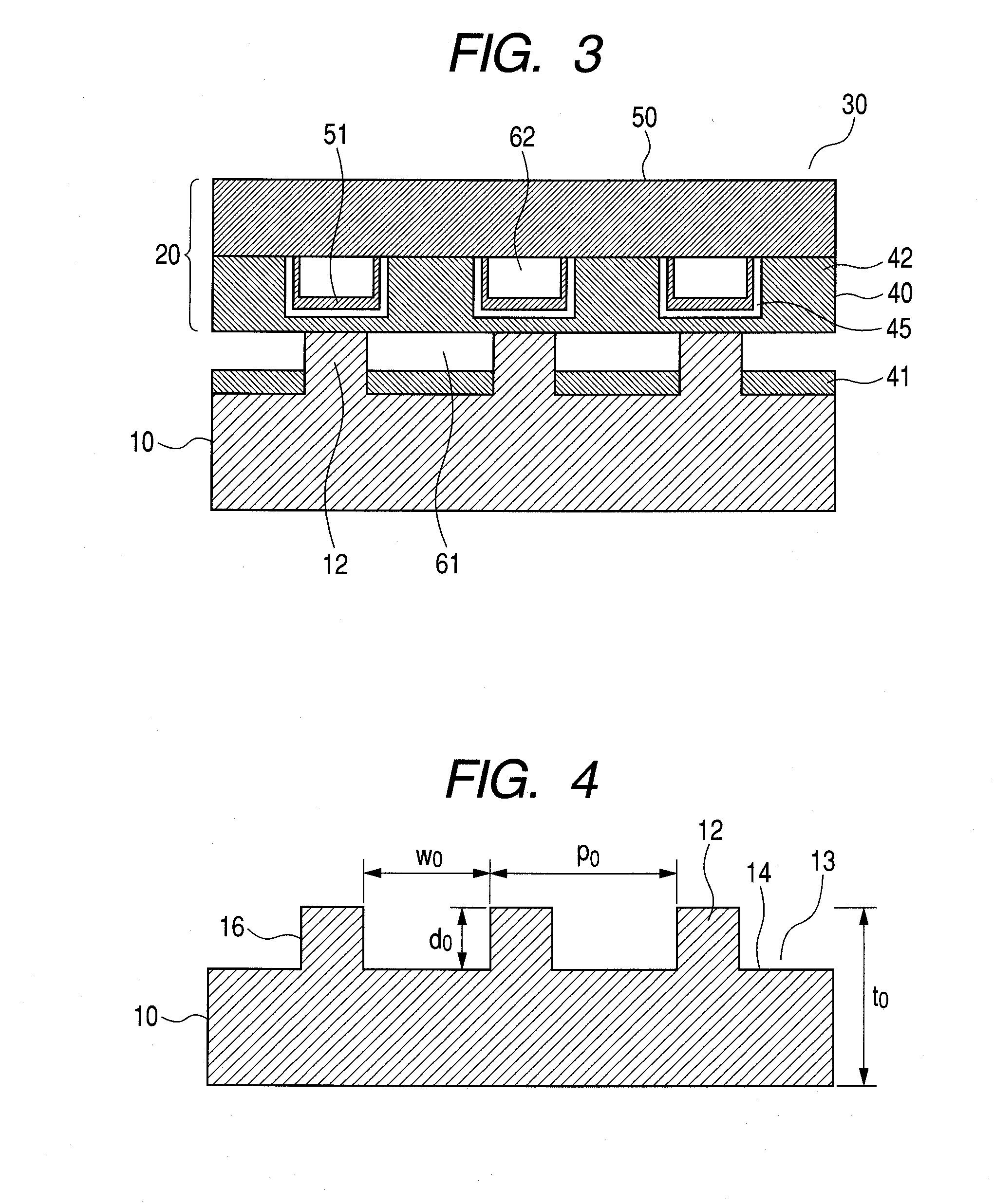
[0140]As a second embodiment of the present invention, an example of the nitride semiconductor-containing composite substrate is described.

[0141]FIG. 3 shows a schematic sectional view for illustrating an example of the nitride semiconductor-containing composite substrate in the present embodiment.

[0142]FIG. 3 illustrates a base substrate 10, a raised portion 12 of the base substrate, a nitride semiconductor-containing composite substrate 30, a nitride semiconductor 41 formed in a recessed portion of the base substrate and a void 61 between the base substrate and the nitride semiconductor.

[0143]The nitride semiconductor-containing composite substrate 30 in the present embodiment is formed of the base substrate 10 and the nitride semiconductor-containing structure 20.

[0144]The base substrate 10 and the structure 20 may be connected to each other without any gap therebetween. When the structure 20 is formed on the base substrate 10 by crystal growth, for the purpose of ensuring the qu...

third embodiment

[0172]As a third embodiment of the present invention, an example of the production method of a nitride semiconductor-containing composite substrate is described.

[0173]FIGS. 5A to 5F shows the schematic sectional views for illustrating an example of the production method of a nitride semiconductor-containing composite substrate in the present embodiment.

[0174]In the production of the composite substrate, first the base substrate 10 is prepared (FIG. 5A).

[0175]The base substrate 10 may be a simple single crystal substrate. The material of the base substrate 10 is, for example, any of a nitride semiconductor typified by GaN, sapphire, silicon (Si) and silicon carbide (SiC).

[0176]In the base substrate 10, according to the intended purpose, on a simple single crystal substrate, an intermediate film (not shown) homogeneous or heterogeneous to the single crystal substrate may be further formed.

[0177]The intermediate film may be a multilayer film. As an example, the intermediate film is a m...


PUM


Abstract

A nitride semiconductor layer-containing structure having a configuration in which: the structure includes a laminated structure based on at least two nitride semiconductor layers; the structure includes between the two nitride semiconductor layers in the laminated structure a plurality of voids surrounded by the faces of the walls inclusive of the inner walls of the recessed portions of the asperity pattern formed on the nitride semiconductor layer that is the lower layer of the two nitride semiconductor layers; and crystallinity defect-containing portions to suppress the lateral growth of the nitride semiconductor layer are formed on at least part of the inner walls of the recessed portions to form the voids.

Description

TECHNICAL FIELD[0001]The present invention relates to a nitride semiconductor layer-containing structure, a nitride semiconductor layer-containing composite substrate and production methods of these. In particular, the present invention relates to a production method of a nitride semiconductor layer based on an epitaxial lateral over growth.BACKGROUND ART[0002]A nitride semiconductor, for example, a gallium nitride compound semiconductor represented by a general formula AlxGayIn1-x-yN (0≦x≦1, 0≦y≦1, 0≦x+y≦1) has a relatively large band gap and is a direct transition type semiconductor material.[0003]Accordingly, nitride semiconductors attract attention as the materials for forming semiconductor light emitting devices such as a semiconductor laser capable of emitting short wavelength light corresponding to from ultraviolet light to green light, and a light emitting diode (LED) capable of covering a wide emission wavelength range from ultraviolet light to red light and additionally wh...

Claims


Application Information

Patent Timeline
IPC IPC(8): H01L21/20H01L29/20
CPCH01L21/02378H01L21/02381H01L21/02389H01L21/0242H01L21/0265H01L21/0254H01L21/0262H01L21/02639H01L21/02458
Inventor WANG, SHINANTAMAMORI, KENJI
Owner CANON KK
Learn More