Eureka AIR delivers breakthrough ideas for toughest innovation challenges, trusted by R&D personnel around the world.

Amorphous oxide semiconductor material, field-effect transistor, and display device

a semiconductor material and field-effect technology, applied in semiconductor devices, organic semiconductor devices, electrical devices, etc., can solve the problems of high manufacturing temperature, difficult to form silicon tfts on flexible substrates, and not shown that a tft having igzo fabricated by these documents as its active layer is sufficien

Active Publication Date: 2011-02-24
SAMSUNG DISPLAY CO LTD
View PDF3 Cites 30 Cited by
  • Summary
  • Abstract
  • Description
  • Claims
  • Application Information

AI Technical Summary

Benefits of technology

[0053]According to the present invention, there can be provided an amorphous oxide semiconductor material where light absorption is reduced with respect to light whose wavelength is in the visible light short-wavelength region of 400 nm to 420 nm.

Problems solved by technology

On the other hand, silicon TFTs, which are currently the mainstream of TFTs that drive displays, have a high manufacturing temperature and it is difficult to form silicon TFTs on flexible substrates.
However, considering that a blue color filter passes about 70% of 400 nm light, that the skirt of the emission spectrum of blue light of an organic EL element continues to 420 nm, and that, thinking about the fabrication of a transparent device, the device is exposed to sunlight, it has not been shown that a TFT having IGZO fabricated by these documents as its active layer is sufficient.
Additionally, these changes in properties have a great affect on stable operation at the time of TFT driving.
However, in the inventions of patent documents 1 and 2, the purpose is to not allow the amorphous IGZO serving as the active layer to be irradiated with light, and there is no description in relation to improving the light irradiation properties of the amorphous IGZO itself.
When this amorphous oxide is used as an active layer of a transistor, it is conceivable that the realization of normally-off is extremely difficult.
However, no experimental data relating to light absorption are shown as examples.
Additionally, a composition range is claimed including also a Ga-rich region with good photostability, but according to the specification, it is necessary for the transistor to take a structure that blocks a semiconducting phase, so it is thought that the optical properties are not good.

Method used


Image

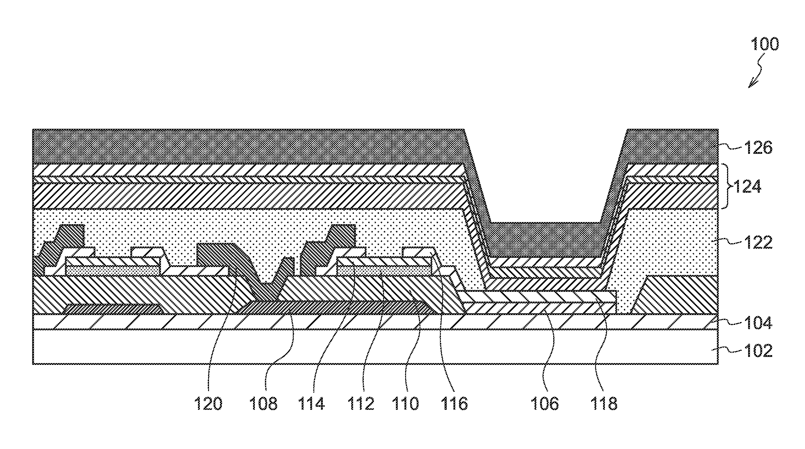
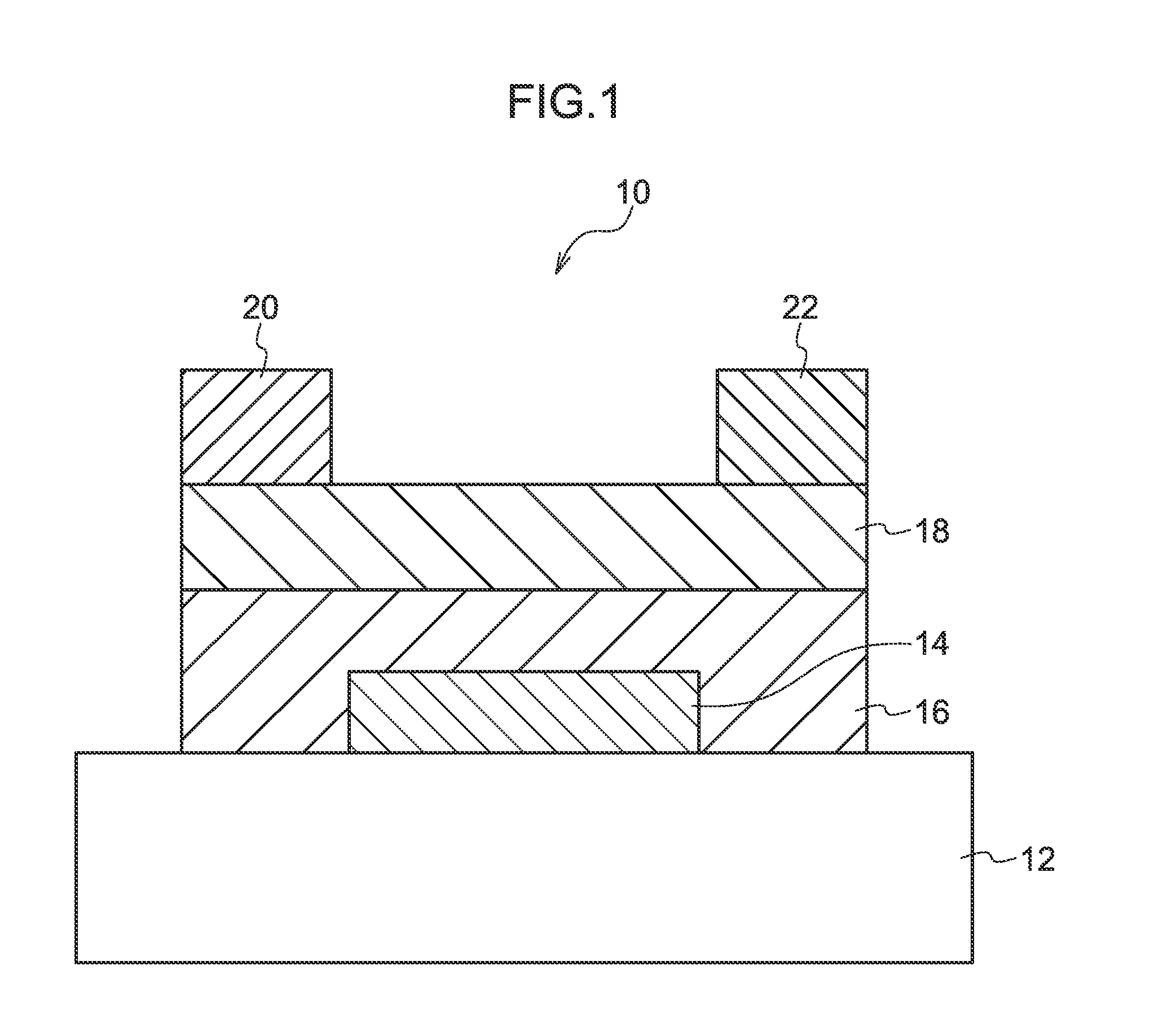
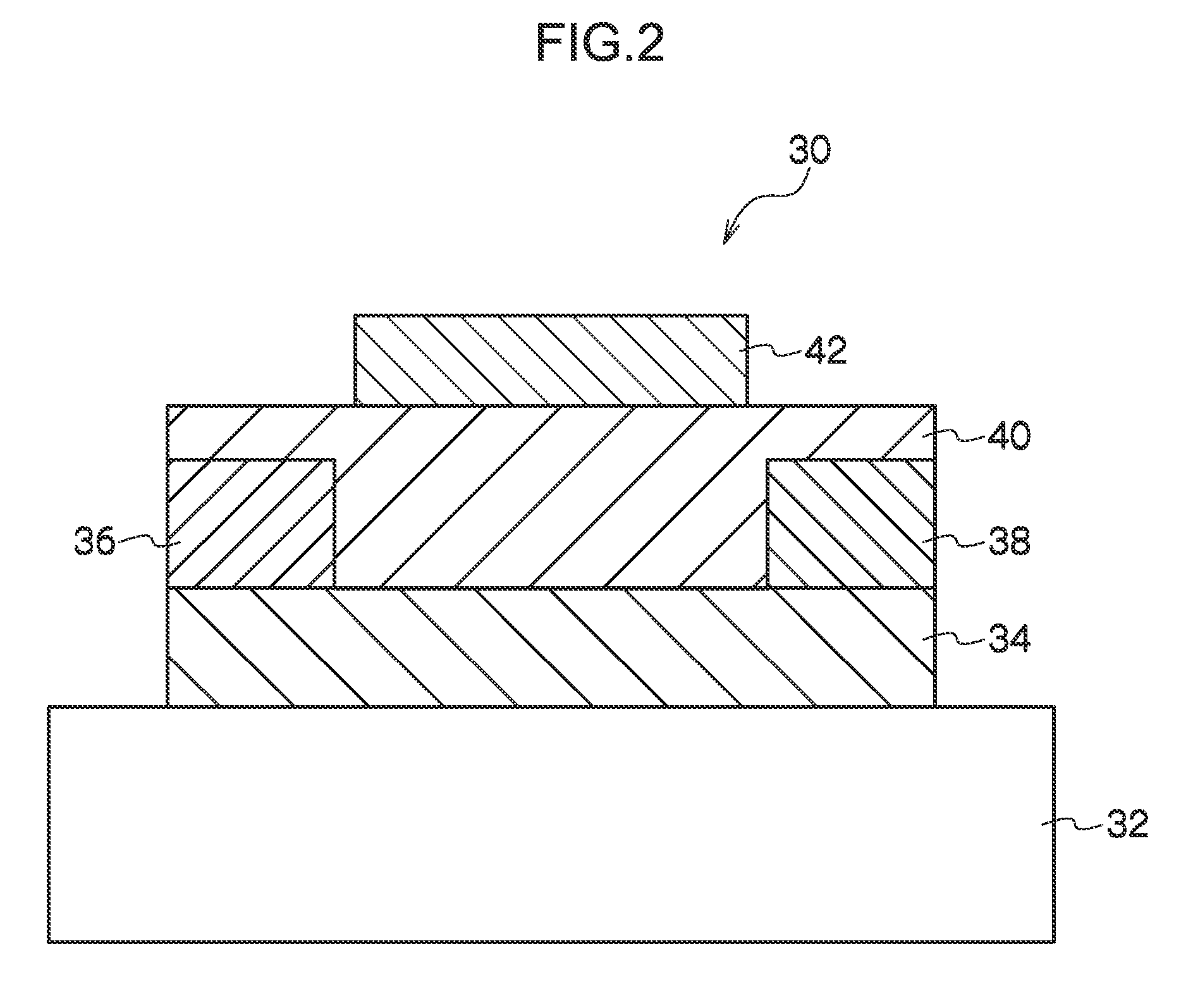
  • Amorphous oxide semiconductor material, field-effect transistor, and display device
  • Amorphous oxide semiconductor material, field-effect transistor, and display device
  • Amorphous oxide semiconductor material, field-effect transistor, and display device

Examples


example 1

[0159]As an amorphous oxide semiconductor material pertaining to example 1 of the present invention, an IGZO film 1 having a composition ratio of In:Ga:Zn=0.7:1.3:1.0 was formed.

[0160]Specifically, the IGZO film 1 pertaining to example 1 was formed on a 25 mm2 quartz glass by co-sputtering resulting from each target of InGaZnO4, ZnO, and Ga2O3. For these targets, targets (99.99% purity) made by Toshima Manufacturing Co., Ltd. were used. When using the InGaZnO4 and Ga2O3 targets, film formation was performed by RF sputtering, and when using the ZnO target, film formation was performed by DC sputtering. When using the ZnO target, generally the resistance of the ZnO is high and film formation is often performed by RF sputtering, but DC sputtering was employed because film formation by DC sputtering was possible and from the standpoint of mass productivity.

example 2

[0161]As an amorphous oxide semiconductor material pertaining to example 2 of the present invention, an IGZO film 2 having a composition ratio of In:Ga:Zn=0.5:1.5:1.0 was formed. This IGZO film 2 was formed using the same film-forming method as in example 1 except that the composition ratio was changed.

example 3

[0162]As an amorphous oxide semiconductor material pertaining to example 3 of the present invention, an IGZO film 3 having a composition ratio of In:Ga:Zn=0.7:1.3:2.0 was formed. This IGZO film 3 was formed using the same film-forming method as in example 1 except that the composition ratio was changed.


PUM

PropertyMeasurementUnit
optical band gapaaaaaaaaaa
threshold voltage Vthaaaaaaaaaa
wavelength peakaaaaaaaaaa

Abstract

There is provided an amorphous oxide semiconductor material including an amorphous oxide semiconductor including In, Ga and Zn, wherein when In:Ga:Zn=a:b:c denotes an element composition ratio of the oxide semiconductor, the element composition ratio is defined by the range of a+b=2 and b<2 and c<4b−3.2 and c>−5b+8 and 1≦c≦2.

Description

CROSS-REFERENCE TO RELATED APPLICATIONS[0001]This application is based on and claims priority under 35 USC 119 from Japanese Patent Application No. 2009-189340 filed on Aug. 18, 2009 and Japanese Patent Application No. 2010-002370 filed on Jan. 7, 2010, the disclosures of which are incorporated by reference herein.BACKGROUND[0002]1. Technical Field[0003]The present invention relates to an amorphous oxide semiconductor material, a field-effect transistor, and a display device.[0004]2. Related Art[0005]Field-effect transistors are widely used as unit elements of integrated circuits for semiconductor memories, high-frequency signal amplifying elements, and elements for driving display elements such as liquid crystal display elements, and transistors that have been made into a thin film are called thin-film transistors (TFT). Additionally, silicon TFTs having an active layer comprising amorphous silicon that is formable in a large area are used in flat panel displays.[0006]In recent yea...

Claims


Application Information

Patent Timeline
Patent Type & Authority Applications(United States)
IPC IPC(8): H01L33/00H01L29/26H01L29/786
CPCH01L27/3248H01L2251/5338H01L29/7869H01L27/3262H01L29/66969H01L29/78693H01L27/1225H10K59/123H10K59/1213H10K2102/311H01L29/26
Inventor HAMA, TAKESHISUZUKI, MASAYUKITANAKA, ATSUSHIMOCHIZUKI, FUMIHIKO
Owner SAMSUNG DISPLAY CO LTD
Why Eureka
Eureka Blog
Learn More