
Process for wet singulation using a dicing moat structure

a technology of wet singulation and moat structure, which is applied in the direction of basic electric elements, semiconductor/solid-state device manufacturing, electrical equipment, etc., can solve the problems of serious reliability problems, mechanically fragile structure comprised of sensitive interfaces which can be easily compromised, and the operation of dicing these thinned structures is even more delicate, so as to reduce the cost of fabrication and scrap, the effect of reducing the size of the chip

Active Publication Date: 2010-10-14
GLOBALFOUNDRIES US INC
View PDF40 Cites 39 Cited by
  • Summary
  • Abstract
  • Description
  • Claims
  • Application Information

AI Technical Summary

Benefits of technology

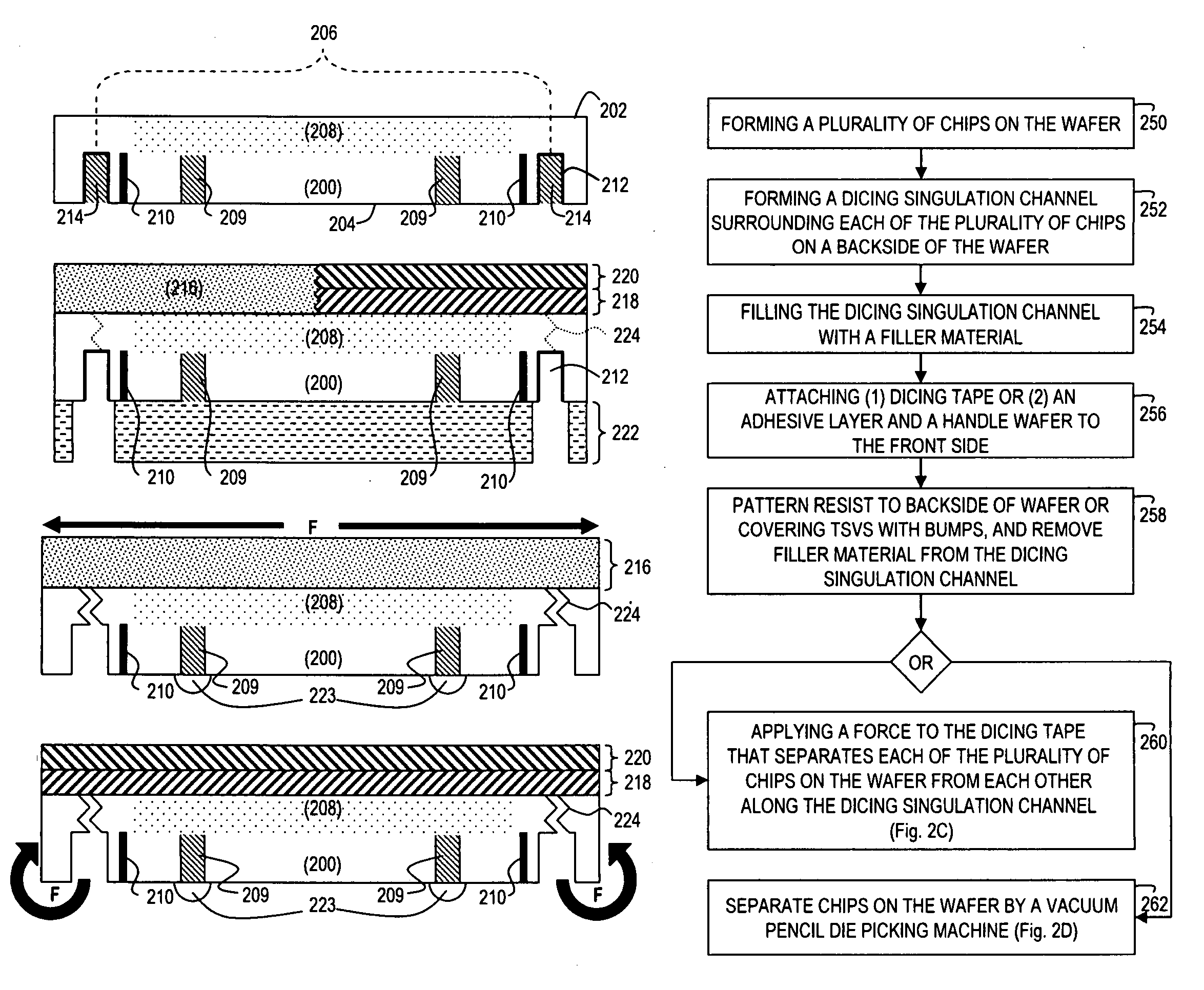
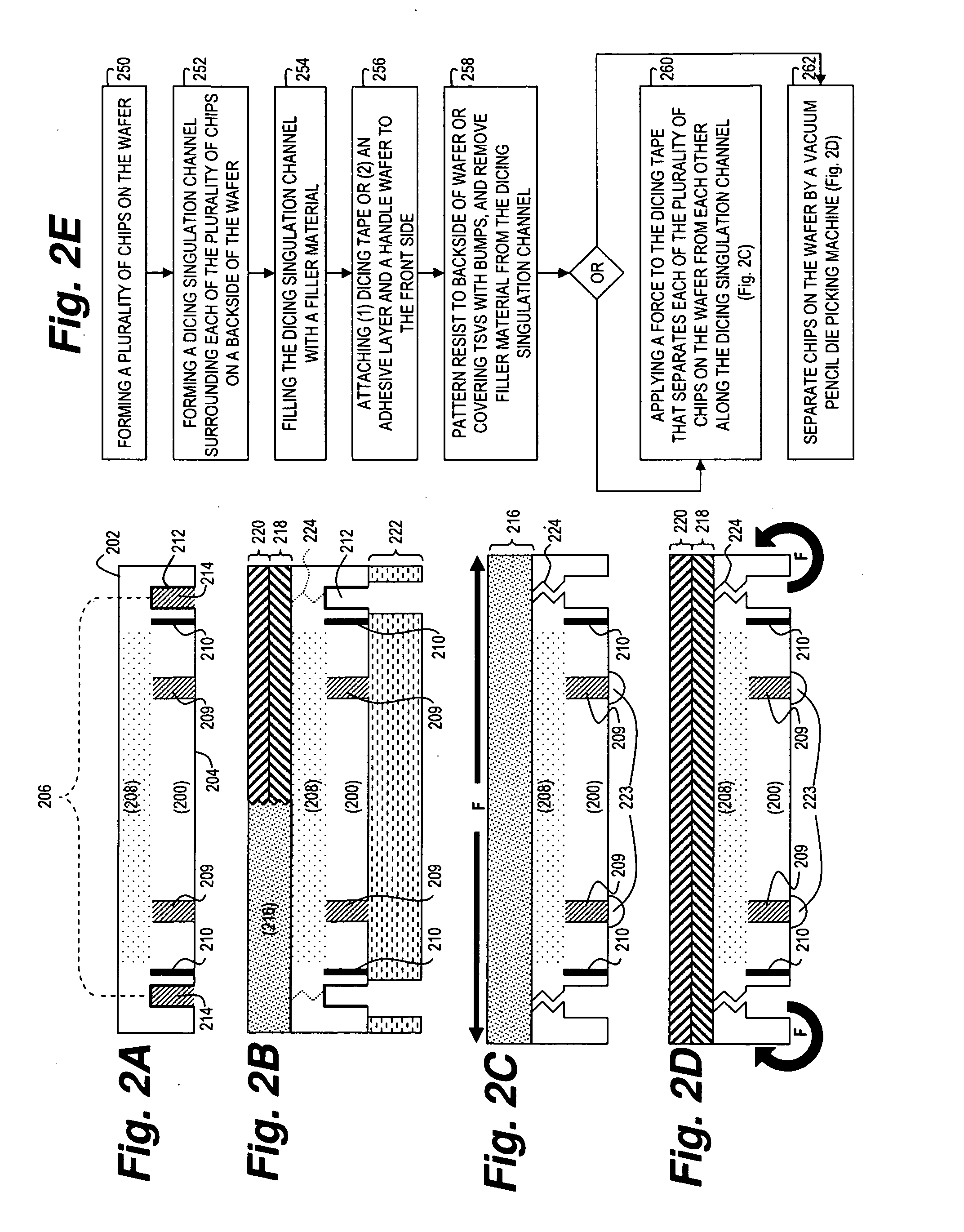
[0009]In view of the foregoing and other exemplary problems, drawbacks, and disadvantages of the conventional methods and structures, the exemplary aspects of the present invention provide an advantage in smaller chip size, less damage due to singulation, lower fabrication and scrap costs, and the elimination for a need for metal crackstop structure.
[0013]With its unique and novel features, the present invention provides an advantage in smaller chip fabrication size, less damage due to singulation, lower fabrication and scrap costs, and the elimination for a need for metal crackstop.

Problems solved by technology

For modern and advanced generation Back-End-Of-The-Line (BEOL) technology products, the integration of copper and Low-K dielectric materials results in a mechanically fragile structure comprised of sensitive interfaces which can be easily compromised by chip edge damage, despite the use of metal-stack crackstop structure.
This can lead to serious reliability problems, particularly in high stress plastic-packaged parts which employ Controlled Collapse Chip Connection (C4) solder connections.
The dicing of these thinned structures is even more delicate an operation than for the full ˜780 μm wafer.
Even so, the attendant reliability risk due to mechanically induced chip edge cracking remains a concern.

Method used


Image

  • Process for wet singulation using a dicing moat structure
  • Process for wet singulation using a dicing moat structure
  • Process for wet singulation using a dicing moat structure

Examples


second embodiment

[0045]FIGS. 3A-3E further illustrates the present invention where a deposition process of tungsten, as shown if FIG. 3A, creates a “seam”302 in the silicon 200 at the dicing singulation channel 300 used to facilitate removal by wet etch in the formation of the empty backside singulation trench 300. Alternatively, the wet etch may be eliminated due to the presence of the seam 302 in the dicing singulation channel 300, especially if the seam material is tungsten. In this instance, bumps 223 cover the TSVs 209 to protect from the backside etching process. The dicing singulation channel 300 is partially filed with the seam material 302 in contrast to the filler material 214 of FIG. 2A. FIG. 3B illustrates that once backside processing of the wafer is complete, the wafer front side 202 is attached to either dicing tape 216 or a combination of an adhesive layer 218 and a handle wafer 220. FIG. 3C illustrates die singulation achieved in a first configuration using a gentle separation force...

third embodiment

[0048]FIGS. 4A-4F illustrate the present invention where the dicing singulation channel 400 filled with filler material 402 (in similar manner to 214 of FIG. 2A) is formed is placed so as to be vertically coincident with a BEOL singulation channel structure 404 proceeding from the front side 202 of the chip. FIG. 4B illustrates the removal of the singulation channel structure 404 and the filler material 402 through a front side wet etch process or any other suitable selective material removal process. Once the front side processing of the wafer is complete, FIG. 4C illustrates the wafer front side 202 is attached to either dicing tape 216 or a combination of an adhesive layer 218 and a handle wafer 220, and the wafer undergoes a backside thinning process to remove material to a level 406 to expose the dicing singulation channel 400 thereby effectively separating each of the chips from the wafer. FIG. 4D illustrates the addition of bumps 223 deposited on TSVs 209 and further separati...

fourth embodiment

[0051]FIGS. 5A-5F illustrate the present invention where the dicing singulation channel 500 is formed between two adjacent through silicon vias (TSVs) 502 adjacent to form a space between the TSVs to be vertically coincident with a BEOL singulation channel structure 504 proceeding from the front side 202 of the chip. FIG. 5B illustrates the removal of the singulation channel structure 504 and the substrate material between the adjacent TSVs 502 through a front side wet etch process or any other suitable selective material removal process. Once the front side processing of the wafer is complete, FIG. 5C illustrates the wafer front side 202 is attached to either dicing tape 216 or a combination of an adhesive layer 218 and a handle wafer 220, and the wafer undergoes a backside thinning process to remove material to a level 506 to expose the dicing singulation channel 500 thereby effectively separating each of the chips from the wafer. FIG. 5D illustrates the addition of bumps 223 depo...


PUM


Abstract

A method includes receiving at least one wafer having a front side and a backside, where the front side has a plurality of integrated circuit chips thereon. The backside of the wafer is thinned, a pattern of material is removed from the backside of the wafer to form a plurality of dicing trenches. Each of the dicing trenches are positioned opposite a location on the front side of the wafer that corresponds to edges of each of the plurality of chips. The dicing trenches are filled with a filler material and a dicing support is attached to a front side of the wafer. The filler material is removed from the dicing trenches, and a force is applied to the dicing support to separate each of the plurality of chips on the wafer from each other along the dicing trenches.

Description

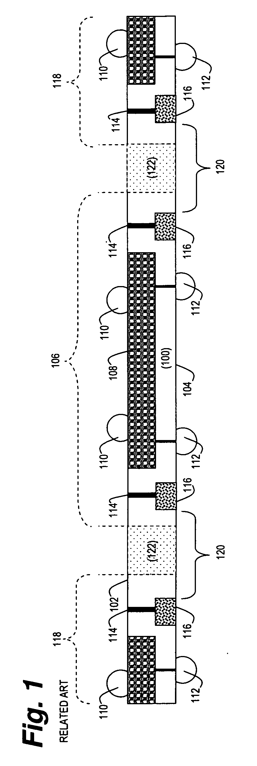
BACKGROUND OF THE INVENTION[0001]1. Field of the Invention[0002]The present invention generally relates to a method for simultaneously dicing a plurality of chips on a wafer to achieve singulation (separation) of semiconductor chip products from parent wafers at the end of the wafer level fabrication process.[0003]2. Description of the Related Art[0004]The industry standard methodology for dicing semiconductor wafers into chips currently involves a mechanical saw that has a blade width that is typically on the order of 50 μm. The mechanical saw can be used alone, or for more advanced technology products, in combination with a laser that cuts an initial scribe line at the edge of each die in an effort to limit the probability of long-range saw-induced crack propagation from the kerf area into the chip edge. For modern and advanced generation Back-End-Of-The-Line (BEOL) technology products, the integration of copper and Low-K dielectric materials results in a mechanically fragile stru...

Claims


Application Information

Patent Timeline
IPC IPC(8): H01L21/78
CPCH01L21/78
Inventor ANDRY, PAUL S.DAUBENSPECK, TIMOTHY H.GAMBINO, JEFFREY P.SPROGIS, EDMUND J.TSANG, CORNELIA K.
Owner GLOBALFOUNDRIES US INC
Learn More