
Optical semiconductor device with a concentration of residual silicon

a technology of optical semiconductor devices and residual si, which is applied in the direction of semiconductor devices, chemistry apparatus and processes, after-treatment, etc., can solve the problems of inability to eliminate residual si of a regrowth interface slow etching rate, and inability to remove residual si in a straightforward manner, so as to improve the performance of the semiconductor device, the effect of stable and reproducible elimination of impurity contamination and physical damage, and the shape chang

Inactive Publication Date: 2010-10-07
NEC CORP
View PDF21 Cites 0 Cited by
  • Summary
  • Abstract
  • Description
  • Claims
  • Application Information

AI Technical Summary

Benefits of technology

[0010]In order to resolve this situation, it is an object of the present invention to provide a semiconductor surface cleaning procedure that does not induce the occurrence of impurity diffusion and crystal defects within the original semiconductor layers, that keeps changes in shape to a minimum, and that stably and reproducibly eliminates impurity contamination and physical damage at a semiconductor substrate surface prior to crystal growth and a semiconductor surface prior to regrowth, and provide an embedded semiconductor laser structure having superior lasing characteristics where increase of IVBA and reduction of ηi due to doping of surplus Zn etc., and crystal defects do not occur.
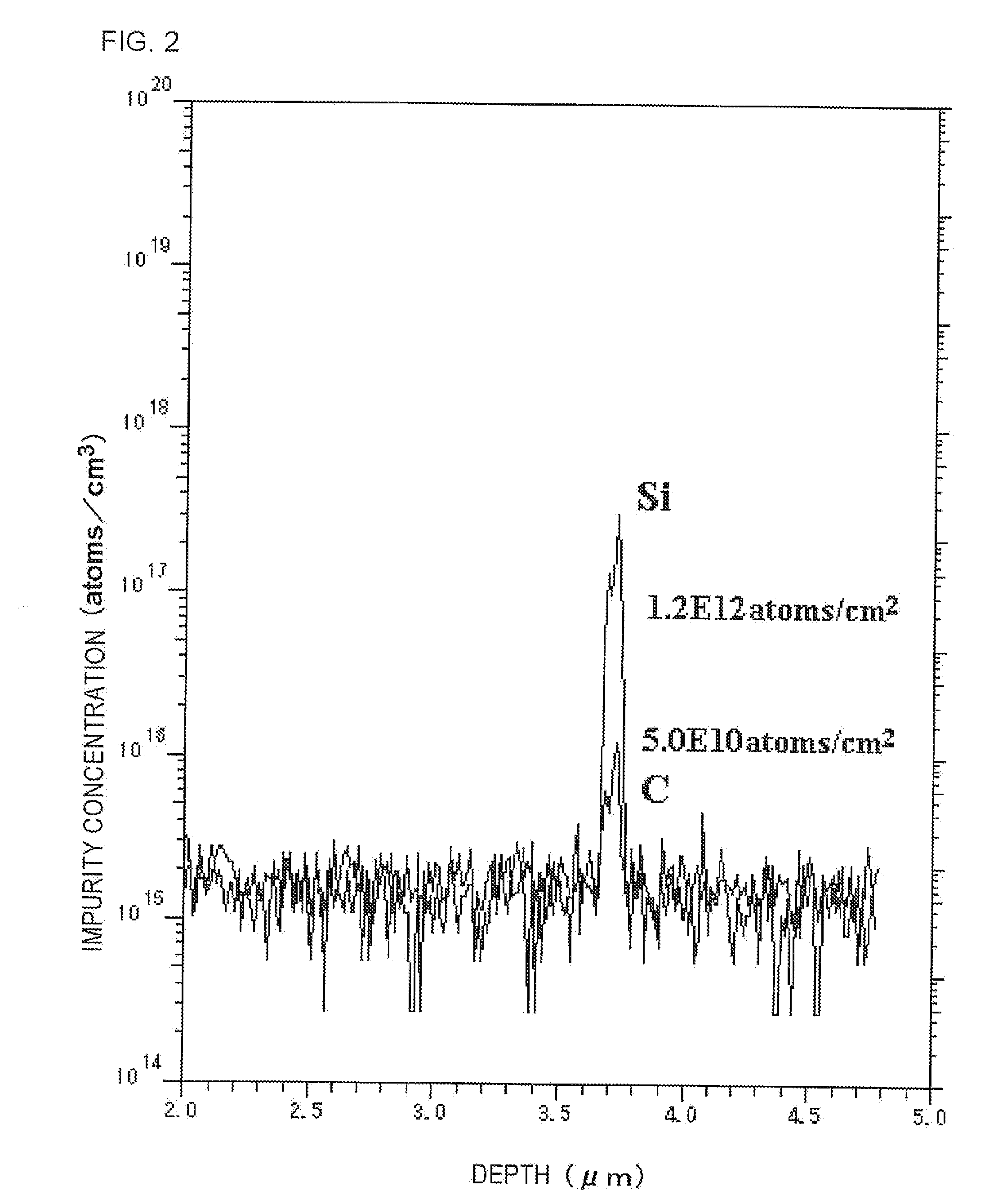
[0062]In a fourth effect, at the optical semiconductor device, concentration of residual Si of the regrowth interface within the cladding layer is 5×10¹¹ atoms / cm2 or less. Leakage current between devices can therefore be suppressed, and it is possible to provide an integrated device in the possession of an embedded semiconductor laser having superior operating characteristics.

Problems solved by technology

However, in the related art, the etching rate is slow compared to the structural elements of the semiconductor crystal and it is easy for contaminants to remain on the surface so that, for example, as published in IEEE Journal of selected Topics in Quantum Electronics, Vol. 3, No. 3, p 845 to p 853, even if an InP surface is etched within a growth chamber using PCl3 as an etching gas, the Si is substantially not etched and remains on the surface.
Further, in the results of evaluation by these inventors, in the vicinity of a normal crystal growth temperature, even if etching is implemented within a crystal growth chamber as shown in U.S. Pat. No. 3,158,651, residual Si of a regrowth interface cannot be eliminated in a straightforward manner.
Moreover, if the substrate temperature is raised too high in order to eliminate the residual Si, if the etching is too deep, impurity diffusion and crystal defects occur within the original semiconductor layer, change in shape occurs due to etching, and it becomes no longer possible to make a device structure as the design intends.
However, even if the bond strength of bonds occurring due to this chemical reaction is relatively weak so that a compound is formed by the contaminant bonding with the etching agent so as to be detached from the semiconductor surface, it is predicted that the contaminant will become reattached to the semiconductor surface directly after breaking of the bonds.
It is therefore predicted that elimination will be difficult because of reattachment of specific contaminant adhered to the semiconductor surface to the semiconductor layer.

Method used


Image

  • Optical semiconductor device with a concentration of residual silicon
  • Optical semiconductor device with a concentration of residual silicon
  • Optical semiconductor device with a concentration of residual silicon

Examples


first embodiment

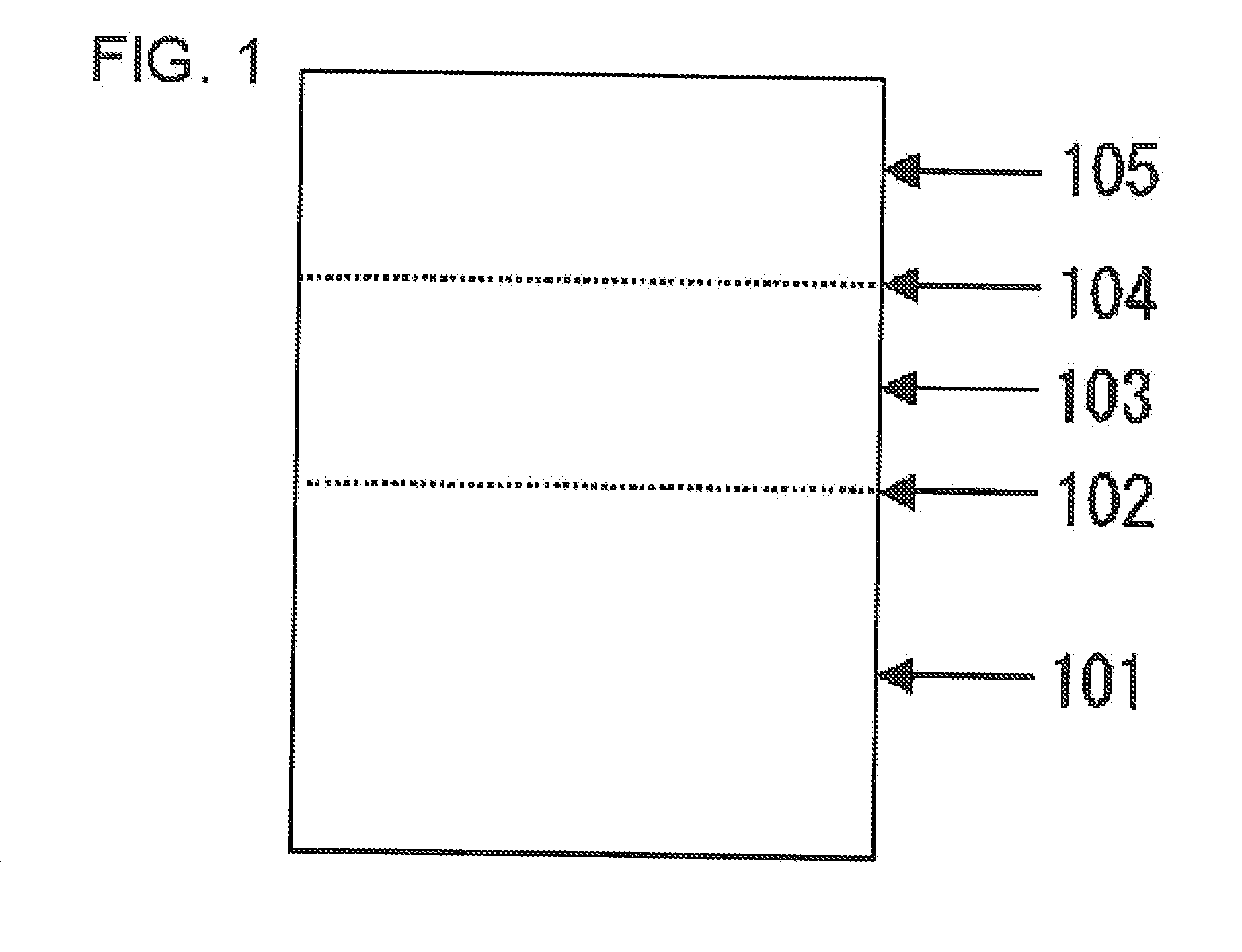
[0096]This embodiment described a residual impurity removal for a growth interface in the case of re-growing InP on InP using MOVPE techniques. Here, t-butyl chloride (TBCl: (CH3)3CCl) is used as the source material having an etching action, and trimethylindium (TMIn) and phosphine (PH3) are used as the crystal growth source material. As shown in FIG. 1, after an undoped InP layer 103 is grown to 1.0 μm as a growth layer for the first time using MOVPE techniques under a low pressure (60 Torr) on the Sn doped {001} InP substrate 101, the wafer is temporarily removed from an MOVPE reactor and is exposed to the atmosphere for twelve hours. Wet chemical treatment etc. is not implemented. After this, the wafer is again moved back into the MOVPE reactor, and an undoped InP layer 105 is regrown to 0.5 μm as the second growth layer.

[0097]At the second growth interface 104 directly before the start of the second growth, in the MOVPE reactor, TBCl, TMIn and PH3 are supplied to the surface of ...

second embodiment

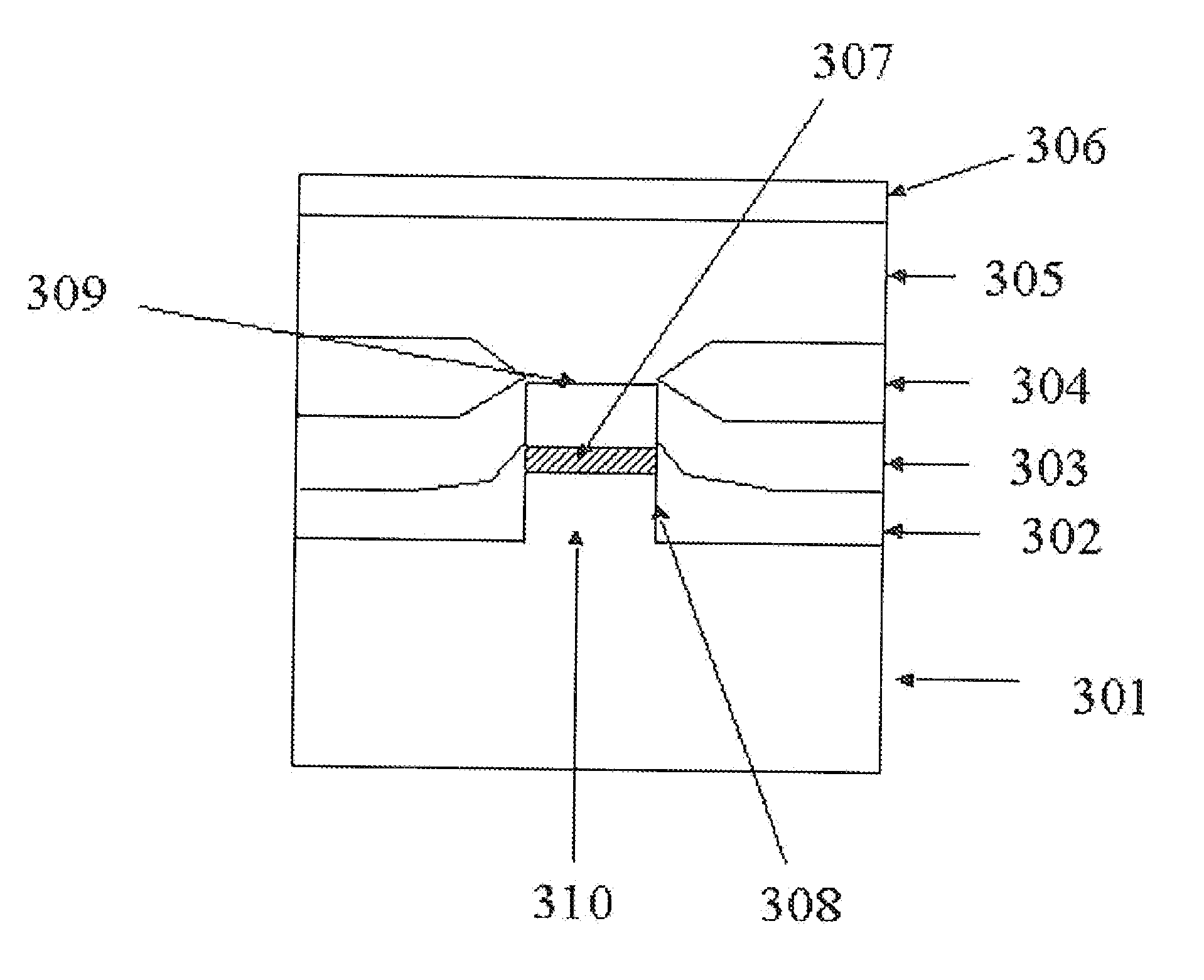
[0102]In this embodiment, the present invention is applied to an InP family semiconductor laser device. In this embodiment, after forming multi-layer films of a semiconductor taking an active layer as an uppermost layer, part of the surface of the active layer is covered with a mask, portions on both sides of the mask are removed by etching, and a mesa stripe is provided. At this stage, after implementing cleaning treatment of the present invention, semiconductor layers are buried at both sides of the mesa. After this, the surface of the mesa is subjected to the cleaning treatment of the present invention and a semiconductor layer of an upper layer is formed. The following is a description with reference to FIG. 10.

[0103]First, using a normal crystal growth process, a InGaAsP / InGaAsP quantum well 307 constituting an active layer with a double hetero structure is made on an n-type InP substrate 301, and a 2 μm mesa stripe 310 is formed to a depth in the order of 2 μm by dry etching u...

third embodiment

[0107]In this embodiment, the semiconductor multi-layer structure is made in the same way as for the first embodiment with the exception that the conditions for cleaning treatment are changed, and the concentration of residual impurities such as C, O and Si at the second growth interface 104 are measured. The conditions for the cleaning treatment are shown in table 1. A description is given in the following of each item in “treatment conditions” of table 1.

(i) Gas Species

[0108]Here, t-butyl chloride (TBCl: (CH3)3CCl), and bis(dimethylamino) phosphine chloride (BDMAPCl: [N(CH3)2]2PCl) are used.

(ii) Gas Flow Rate

[0109]Amount of gas supplied to the MOVPE reactor is shown.

(iii) Etching Rate

[0110]The etching rate in the case of only supplying etching gas at the flow rates shown in the table is shown. This value is obtained through pre-testing.

(iv) Growth Rate

[0111]The growth rate in the case of only supplying growth gas at the flow rates shown in the table is shown. This value is obtaine...


PUM

PropertyMeasurementUnit
thicknessaaaaaaaaaa
temperatureaaaaaaaaaa
thickness indexaaaaaaaaaa

Abstract

In a crystal growth reactor, a source material having an etching action and a crystal growth source material are simultaneously supplied to a semiconductor wafer surface, so that residual impurities can be eliminated in an efficient manner by balancing etching rate and crystal growth rate.

Description

TECHNICAL FIELD[0001]The present invention relates to technology for cleaning the surface of a semiconductor layer.BACKGROUND ART[0002]In processes for manufacturing a semiconductor device, situations where a step of growing crystal of a semiconductor layer of the same species or different species on a semiconductor substrate, a step of patterning using photolithography taking a dielectric body etc. as a mask and performing chemical etching or dry etching, and a step of regrowing a semiconductor layer of the same species or a different species in order to bring about a current block structure or an optical confinement structure are repeated are common. In this event, the substrate surface prior to crystal growth and the semiconductor growth layer surface prior to regrowth are easily subjected to contamination with impurities and physical damage due to processes such as exposure to the atmosphere, etching, and cleaning, etc. so that if crystal growth is carried out with these surface...

Claims


Application Information

Patent Timeline
Patent Type & Authority Applications(United States)
IPC IPC(8): H01L29/30C30B33/00H01L21/205H01L21/306
CPCC30B33/00H01L21/02046H01L21/02392H01L21/02661H01L21/02543H01L21/0262H01L21/02461
Inventor NANIWAE, KOICHI
Owner NEC CORP
Learn More