Functional molecular element, process for producing the same and functional molecular device

Inactive Publication Date: 2010-09-30
SONY CORP
View PDF5 Cites 2 Cited by
  • Summary
  • Abstract
  • Description
  • Claims
  • Application Information

AI Technical Summary

Benefits of technology

[0040]According to the functional molecular elements of the present invention, the π-electron conjugated molecule is formed to have the side chain moiety linked to the skeleton moiety having the substantially planar structure composed of the π-electron conjugated system. Therefore, in the adsorbate molecule, a structure can be obtained in which the side chain moiety is adsorbed on the electrode, whereby the substantially planar structure of the skeleton moiety is disposed substantially parallel to the electrode, and is closely adhered to the electrode. Consequently, the electrical interaction between π-electrons constituting the π-electron conjugated system and the electrode is improved, and the contact resistance between the π-electron conjugated molecule and the electrode is reduced to a low level.
[0042]In view of this, the present inventors made earnest investigations. As a result of their investigations, they succeeded in obtaining the first functional molecular element having a bias voltage region in which a negative differential resistance is exhibited at room temperature, and the second functional molecule in which the bulk electric conductivity obtained by conversion from the current-voltage characteristic of the functional molecular element is not less than 0.1 S / cm, and have come to complete the present invention. It has been found that the two functional molecules having specific conductivities can be distinctly produced easily by using the same π-electron conjugated molecule and simply changing the solvent, in the above-mentioned process for producing the functional molecular element according to the present invention.
[0043]In the functional molecular device according to the present invention, the control electrode for controlling the current by applying an electric field to the first functional molecular element is provided along the stacking direction of the above-mentioned structure. Therefore, it is possible to configure a functional molecular device exhibiting a negative differential resistance (NDR) at room temperature, so that there is a possibility that new kinds of molecular switches and molecular computers may be configured successfully.

Problems solved by technology

Although atoms and molecules can be manipulated, however, it is impractical to make or assemble a new material or a new device by manipulating a huge number of atoms or molecules one by one.
In addition, an increase in the rate of integration of transistors may cause the amount of heat generated per semiconductor chip to be too large, possibly resulting in malfunctions of the semiconductor chips heated to high temperatures or thermal breakage of the chips.
Furthermore, specialists predict that if miniaturization of chips is further advanced in the semiconductor industry, the equipment cost and process cost will expand, and, due also to worsening of yield, the industry may become non-payable at around 2015.
Recently, the problem of the minute irregularities in pattern edges, or of the line edge roughness, has been pointed out as a still graver problem.
In relation to the irregularities in the resist mask surface, it is said that as the pattern miniaturization is advanced, the size of the molecules constituting the resist, the diffusion distance of acid in a chemically amplified photoresist, and the like will be problems.
), and limited ones of the researches concerned those devices which are driven by an electric field.
The above-mentioned problem of line edge roughness is again a serious problem even in these molecular devices, and the problem is considered to become more conspicuous as pattern miniaturization progresses.
However, the problem involved in the electrical connection by linking between the thiol group and the gold electrode is that, whatever good electrical characteristics the molecule itself may have, the connection part between its thiol group end and the electrode has a high electric resistance, and the high electric resistance restricts enhancement of the characteristics of the molecular device (See J. M. Wessels, H. G. Nothofer, W. E. Ford, F. von Wrochem, F. Scholz, T. Vossmeyer, A. Schroedter, H. Weller and A. Yasuda, “Optical and electrical properties of three-dimensional interlinked gold nanoparticle assemblies,” Journal of the American Chemical Society, 126 (10), 3349-3356, Mar. 17, 2004.).

Method used


Image

  • Functional molecular element, process for producing the same and functional molecular device
  • Functional molecular element, process for producing the same and functional molecular device
  • Functional molecular element, process for producing the same and functional molecular device

Examples


embodiment 1

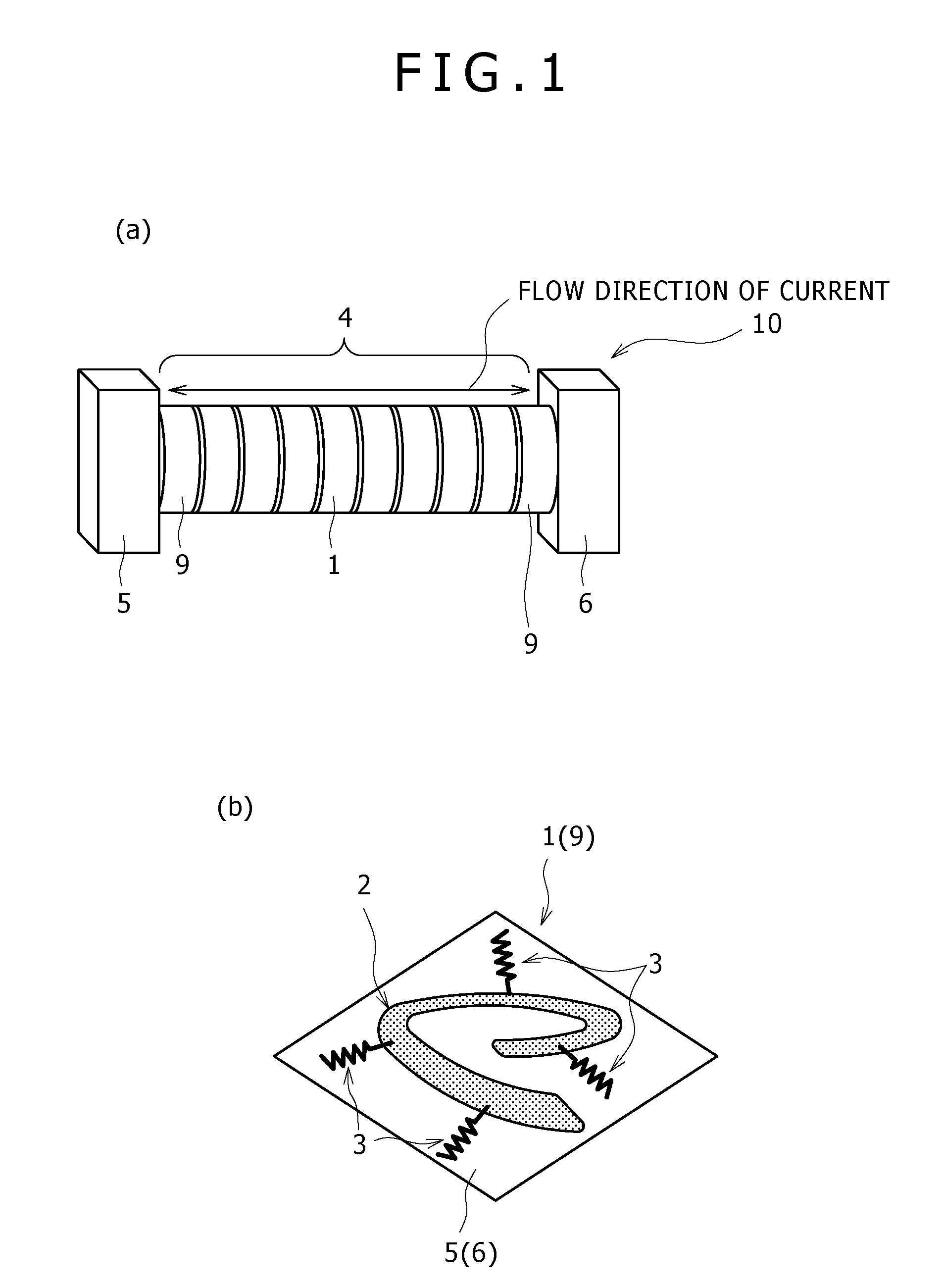
[0068]In Embodiment 1, an example of the functional molecular element corresponding mainly to claims 1 and 2 and claims 16 and 17 will be described.

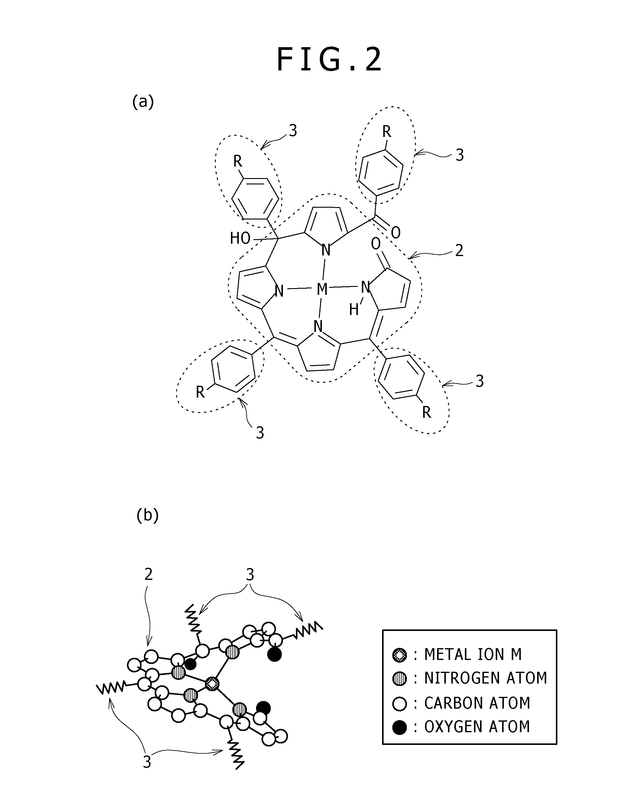
[0069]In (a) of FIG. 2, there is shown the structural formula of one example of molecular structure of a π-electron conjugated molecule 1 constituting the above-mentioned array structure in Embodiment 1. In (b) of FIG. 2, there is shown a schematic illustration for showing mainly the stereostructure of a substantially disk-shaped skeleton moiety 2 of the π-electron conjugated molecule 1 shown in (a) of FIG. 2. In (b) of FIG. 2, a metal ion M, nitrogen atoms, carbon atoms and oxygen atoms constituting the skeleton moiety 2 are shown as spheres, while hydrogen atoms are omitted, and side chain moieties 3 are shown in an extremely simplified or omitted form.

[0070]As shown in (a) and (b) of FIG. 2, the skeleton moiety 2 of the π-electron conjugated molecule 1 has biladienone (specifically, 4,9-biladien-1-one) as its fundamental structure. Bi...

embodiment 2

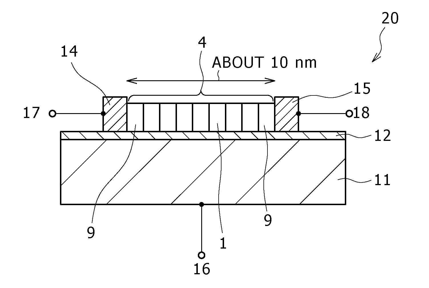
[0083]In Embodiment 2, as an example of a functional molecular device corresponding mainly to claims 14 and 15, a functional molecular device will be described in which the functional molecular element 10 described in Embodiment 1 above is formed between opposed electrodes and which is configured as an insulated gate field effect transistor. FIG. 3 is a sectional view for illustrating the structure of an insulated gate field effect transistor 20 in the present embodiment.

[0084]As shown in FIG. 3, in the insulated gate field effect transistor 20, a doped silicon substrate 11 serves also as a gate electrode 13, which is the above-mentioned control electrode. A silicon oxide layer as a gate insulating film 12 is formed on the surface of the silicon substrate 11. A source electrode 14 and a drain electrode 15 which are composed of gold, for example, are formed on the silicon oxide layer as the above-mentioned opposed electrodes, and the array structure 4 described in Embodiment 1 is dis...

example

[0091]Now, examples of the present invention will be described in detail below.

[0092]In (a) of FIG. 4, there is shown the structural formula of a π-electron conjugated molecule 7 (corresponding to the above-mentioned π-electron conjugated molecule 1) having a substantially disk-shaped skeleton moiety 2 which is used for producing the functional molecular element 10 in the present examples. In (b) and (c) of FIG. 4, there are shown the structural formulas of 4-pentyl-4′-cyanobiphenyl (5CB) and tetrahydrofuran (THF), which are solvents used in producing the functional molecular elements 10. The π-electron conjugated molecule 7 is a zinc complex of a biladienone derivative which has a phenyl group with a dodecyl group —C12H25 linked thereto at the para position, as each of flexible side chain moieties 3.

[0093]For correct evaluation of the characteristics of the functional molecular element 10, the functional molecular element 10 should be produced with good reproducibility. For this pu...


PUM


Abstract

A functional molecular element having a structure in which the contact resistance at the interface between a constituting molecule and an electrode can be reduced, the functional molecular element having a specific conductivity, a process for producing the same, and a functional molecular device, are provided. A π-electron conjugated molecule 1, which is one species of linear tetrapyrrole having a substantially disk-shaped central skeleton moiety 2 and a flexible side chain moiety 3 composed of an alkyl group, is dissolved in 4-pentyl-4′-cyanobiphenyl or tetrahydrofuran, and the concentration is adjusted to an appropriate level. This solution is applied to electrodes 5 and 6, and the solvent is evaporated, whereby an array structure 4 of the π-electron conjugated molecules 1 is self-organizingly formed. An adsorbate molecule 9 in the first layer of the array structure 4 is fixed in such a manner that its side chain moiety 3 is adsorbed on a surface of the electrode 5 or 6 and a substantial disk plane of the skeleton moiety 2 is parallel to and adhered to the surface of the electrode 5 or 6. The stacking direction of the π-electron conjugated molecules 1 in the second and subsequent layers of the array structure 4 is controlled by the π-π interaction between the substantially disk-shaped central skeleton moieties 2.

Description

TECHNICAL FIELD[0001]The present invention relates to a functional molecular element having a specific conductivity, a process for producing the same, and a functional molecular device.BACKGROUND ART[0002]Nanotechnology is a technology for observation, production and use of fine structures of about 10 billionths of meter (10−8 m=10 nm) in size.[0003]In the latter half of the nineteen eighties, an ultrahigh-precision microscope called scanning tunneling microscope was invented, making it possible to look at a single atom and a single molecule. The use of the scanning tunneling microscope makes it possible not only to observe atoms and molecules but also to manipulate them one by one.[0004]For example, an example in which atoms are arranged on a surface of a crystal to draw characters and the like examples have been reported. Although atoms and molecules can be manipulated, however, it is impractical to make or assemble a new material or a new device by manipulating a huge number of a...

Claims


Application Information

Patent Timeline
IPC IPC(8): G05F3/02H01L51/30H01L51/40
CPCB82Y10/00H01L51/0084H01L51/0595H01L51/0512H01L51/0575H01L51/0092H10K85/341H10K85/381H10K10/462H10K10/20H10K10/701H01L29/06H10K10/00
Inventor MATSUI, ERIKOKEUM, CHANGDAEKITA, KOJIROHATAZAWA, TSUYONOBU
Owner SONY CORP
Why Eureka
Try Eureka