Group III-V nitride based semiconductor substrate and method of making same
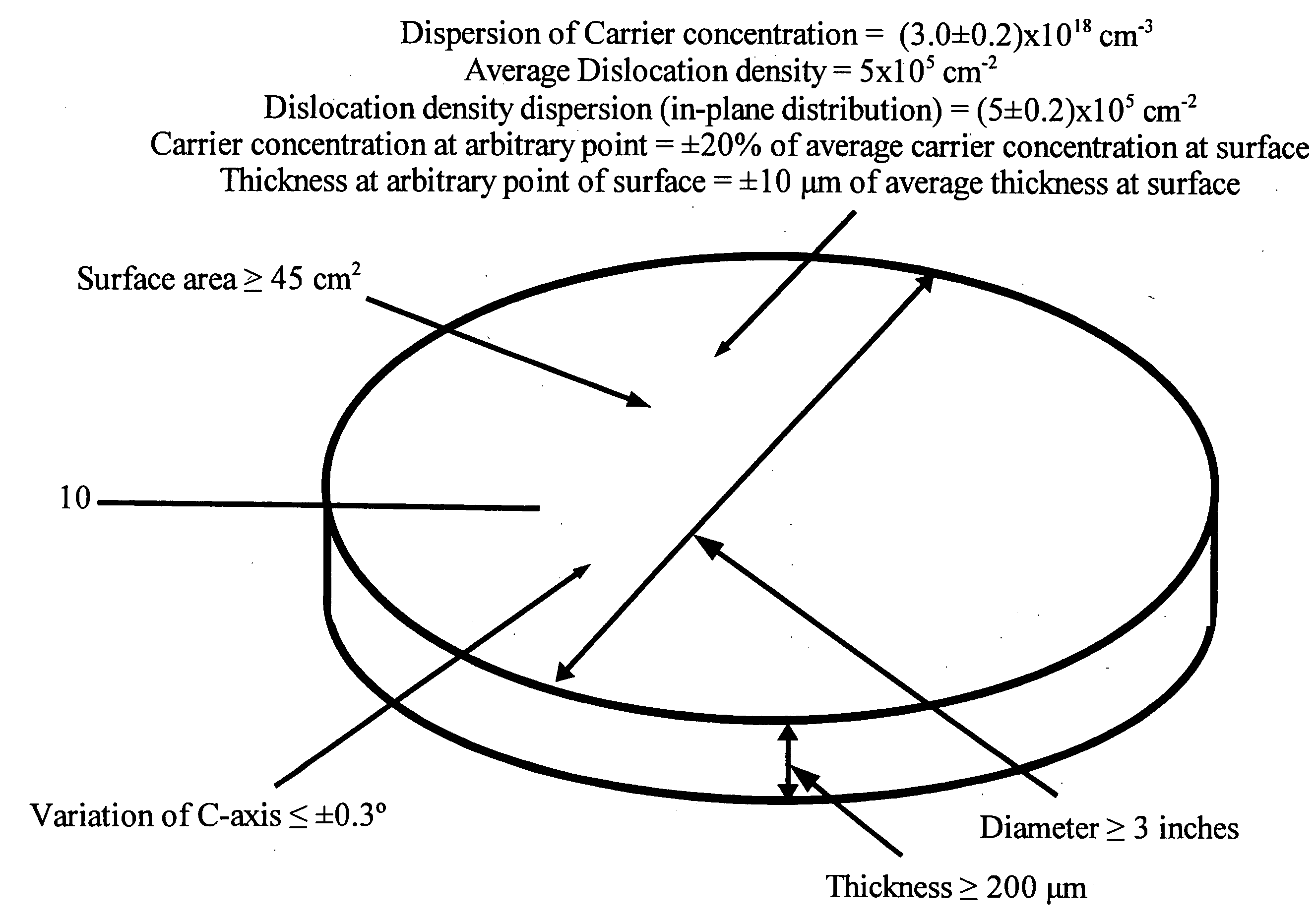
a technology of nitride and semiconductor substrate, which is applied in the direction of crystal growth process, polycrystalline material growth, chemically reactive gas growth, etc., can solve the problems of non-uniform carrier concentration and electrical resistivity, non-uniform in-plane polishing speed, etc., and achieves high uniformity, large surface area, and economic advantages.
- Summary
- Abstract
- Description
- Claims
- Application Information
AI Technical Summary
Benefits of technology
Problems solved by technology
Method used
Image
Examples
##ventive example 1
Inventive Example 1
Preventing the Warping by a Thick Sapphire
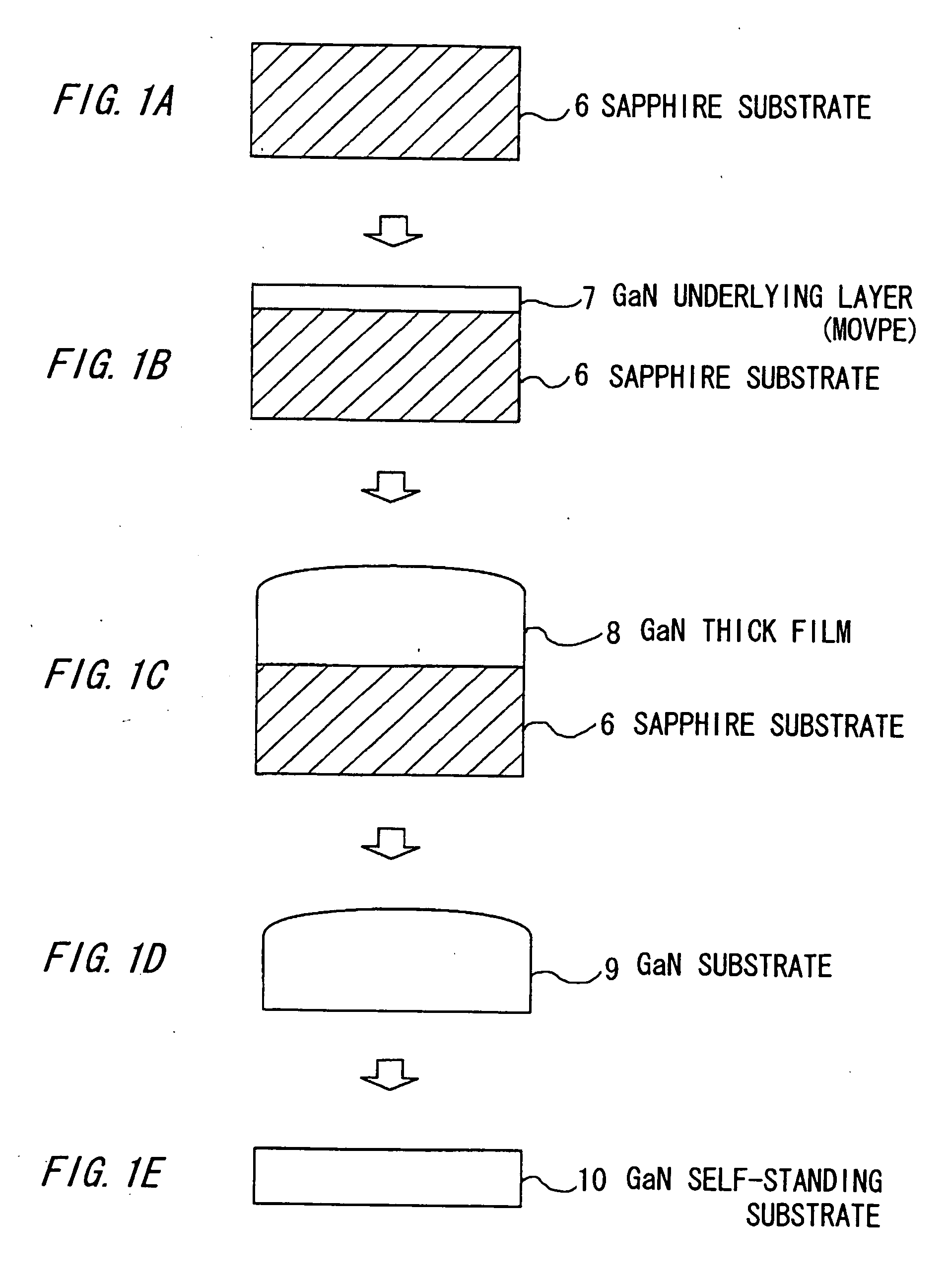
[0088]FIGS. 1A to 1E are illustrative cross sectional views showing of a method of making a group III-V nitride semiconductor substrate in the first exemplary embodiment according to the invention.
[0089]As shown in FIGS. 1A and 1B, a 300 nm thick GaN underlying layer 7 is formed on a c-face sapphire substrate 6 with a diameter of 7.62 cm (=3 inches) and a thickness of 650 μm by MOVPE.
[0090]Then, like the conventional example, it is placed in a HVPE furnace and a Si-doped GaN thick film 8 is grown (FIG. 1C). Carrier gas is N2:H2=1:1. Partial pressures are GaCl=9×10⁻³ atm, NH3=1×10⁻¹ atm. For n-type doping, SiH2Cl2 gas is flown at partial pressure of 5×10⁻⁴ atm. Growth temperature is 1070° C.
[0091]By irradiating YAG laser from the backside of the sapphire substrate 6, a GaN substrate 9 is separated decomposing a GaN crystal at the interface (FIG. 1D).
[0092]The resultant GaN crystal (i.e., GaN thick film 8) has a thickness of...
##ventive example 2
Inventive Example 2
Further Enhancing the Uniformity by Coating Carbon on the Back Face of the Sapphire Substrate
[0095]In the inventive example 1, an about 1 μm thick carbon layer is formed on the back face of the sapphire substrate 6 and then the HVPE growth is conducted in like manner. Thereby, the temperature distribution during growth can be further improved. As is shown in FIG. 1G, the thickness distribution as grown is 800 μm at the central portion and 750 μm at the outermost portion.
[0096]As is also shown in FIG. 1G, the properties of the GaN substrate are also improved. The dislocation density is 1×107 cm−2 both at the central portion and at the outermost portion. At an arbitrary point of a surface of the substrate, a carrier concentration falls within ±20% of an average carrier concentration at the surface. The carrier concentration is 1×1018 cm−3 both at the central portion and at the outermost portion. Further, a dispersion in crystal axis of the surface of the substrate i...
##ventive example 3
Inventive Example 3
Bonding the Sapphire Substrate to the Susceptor+VAS Method
[0097]FIGS. 2A to 2E are illustrative cross sectional views showing of a method of making a group III-V nitride semiconductor substrate in the third exemplary embodiment according to the invention.
[0098]As shown in FIG. 2A, a c-face sapphire substrate 6 with a diameter of 7.62 cm (=3 inches) and a thickness of 330 μm is provided.
[0099]Then, a 300 nm thick GaN thin film (=GaN under lying layer 17) is formed on the sapphire substrate 6. Then, a 20 nm thick Ti layer is formed thereon in vacuum deposition. Then, it is thermally treated in carrier gas of H2:NH3=4:1 at 1060° C. for 30 min. Thereby, the Ti layer is nitrided into a TiN layer and formed into mesh-like structure (i.e., TiN nano-mask 11) with a number of fine holes of tens of nanometers. On the other hand, the GaN underlying layer 17 is etched to have therein voids reaching up to the sapphire substrate 6 (FIG. 2B).
[0100]Then, the void-formed substrate...
PUM
| Property | Measurement | Unit |
|---|---|---|
| surface area | aaaaa | aaaaa |
| thickness | aaaaa | aaaaa |
| thickness | aaaaa | aaaaa |
Abstract
Description
Claims
Application Information
 - R&D
- Intellectual Property
- Life Sciences
- Materials
- Tech Scout
- Unparalleled Data Quality
- Higher Quality Content
- 60% Fewer Hallucinations
Browse by: Latest US Patents, China's latest patents, Technical Efficacy Thesaurus, Application Domain, Technology Topic, Popular Technical Reports.
© 2025 PatSnap. All rights reserved.Legal|Privacy policy|Modern Slavery Act Transparency Statement|Sitemap|About US| Contact US: help@patsnap.com


