
Heat treatment apparatus and method for heating substrate by photo-irradiation

Active Publication Date: 2010-05-06
SCREEN HLDG CO LTD
View PDF11 Cites 30 Cited by
  • Summary
  • Abstract
  • Description
  • Claims
  • Application Information

AI Technical Summary

Benefits of technology

[0012]Since intense irradiation with a higher peak is applied after the execution of the preliminary heating of a substrate with a relatively low light-emission output, it is possible to further increase the surface temperature of the substrate while preventing the substrate from shattering.
[0044]An object of the present invention is thus to further increase the surface temperature of a substrate while preventing the substrate from shattering.

Problems solved by technology

The occurrence of such a phenomenon gives rise to the apprehension that the junction may become deeper than the desired level, hindering good device formation.
However, in order to further increase the ultimate surface temperature of a semiconductor wafer with the emission of flashes of light from flash lamps, it is necessary to emit flashes of light with greater irradiation energy within an extremely short period of time, which must result in an increase in the loads of both flash lamps and their driving circuits.
Consequently, there is also a problem of shortening the lifetimes of such flash lamps.
Another problem also arises in that if flashes of light with a huge irradiation energy are emitted for an extremely short period of time so that the surface temperature of a semiconductor wafer is significantly increased instantaneously, sudden thermal expansion may occur only on the wafer surface, causing the semiconductor wafer to shatter.

Method used


Image

  • Heat treatment apparatus and method for heating substrate by photo-irradiation
  • Heat treatment apparatus and method for heating substrate by photo-irradiation
  • Heat treatment apparatus and method for heating substrate by photo-irradiation

Examples


first preferred embodiment

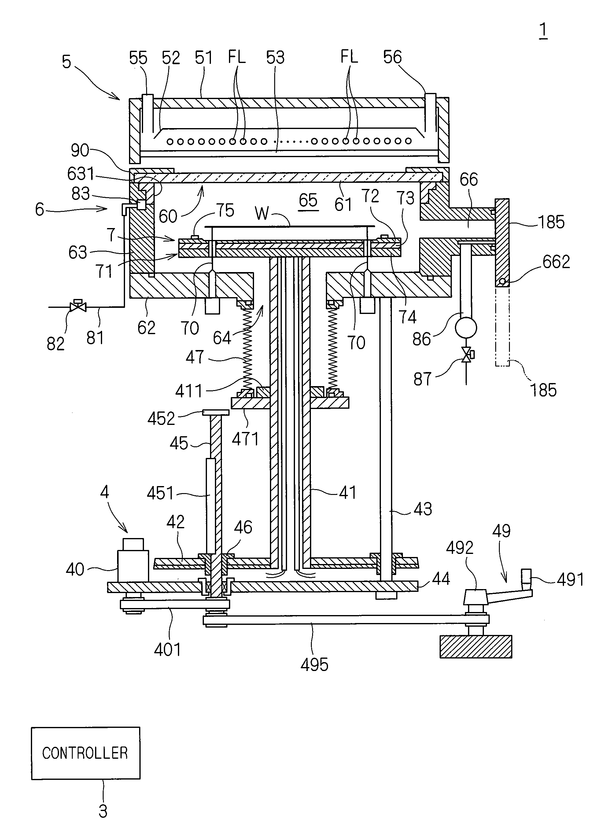
[0068]First, a general configuration of a heat treatment apparatus according to the invention is outlined. FIG. 1 illustrates a longitudinal section of a configuration of a heat treatment apparatus 1 according to the invention. The heat treatment apparatus 1 is a lamp annealer for applying light to a generally disc-shaped semiconductor wafer W serving as a substrate so as to heat the semiconductor wafer W.

[0069]The heat treatment apparatus 1 includes a generally cylindrical chamber 6 for receiving a semiconductor wafer W therein; and a lamp house 5 including a plurality of built-in flash lamps FL. The heat treatment apparatus 1 further includes a controller 3 for controlling each operating mechanism provided in the chamber 6 and in the lamp house 5 for the implementation of the heat treatment of a semiconductor wafer W.

[0070]The chamber 6 is located below the lamp house 5 and includes a chamber side portion 63 having a generally cylindrical inner wall and a chamber bottom portion 62...

second preferred embodiment

[0122]Next, a second preferred embodiment of the present invention will be described. A heat treatment apparatus according to the second preferred embodiment is identical in configuration to that of the first preferred embodiment. The procedure for processing a semiconductor wafer W according to the second preferred embodiment is also generally the same as that in the first preferred embodiment. FIG. 12 shows another example of the correlation between a pulse signal waveform and a current flowing through a circuit. In the second preferred embodiment, the pulse generator 31 outputs a pulse signal having a waveform as shown in the upper part of FIG. 12. The pulse waveform shown in the upper part of FIG. 12 includes a plurality of relatively short pulses PD in the earlier section, then a plurality of pulses PE, and then a single relatively long pulse PF. In the second preferred embodiment, a pulse signal having a waveform as shown in the upper part of FIG. 12 is applied to the gate of ...

third preferred embodiment

[0137]Next, a third preferred embodiment of the present invention will be described. A heat treatment apparatus of the third preferred embodiment is identical in configuration to that of the first preferred embodiment. The procedure for processing a semiconductor wafer W according to the third preferred embodiment is also generally the same as that in the first preferred embodiment. The third preferred embodiment differs from the first preferred embodiment in the output waveform of the light-emission output of a flash lamp FL. FIG. 14 shows a profile of the light-emission output of a flash lamp FL according to the third preferred embodiment. The light-emission output of a flash lamp FL is almost proportional to the current flowing through the flash lamp FL, so that the profile of the light-emission output of a flash lamp FL can be controlled by controlling the waveform of a pulse signal that is output to the gate of the switching element 96.

[0138]The output waveform of light shown i...


PUM


Abstract

Two-step photo-irradiation heat treatment is performed so that a total photo-irradiation time is not more than one second and that a first step of photo-irradiation of a semiconductor wafer is performed with a light-emission output that averages out at a first light-emission output and a second step of photo-irradiation of the semiconductor wafer is performed in accordance with an output waveform that peaks at a second light-emission output that is higher than both average and maximum light-emission outputs in the first step. Performing preliminary photo-irradiation with a relatively low light-emission output in the first step and then performing intense photo-irradiation with a higher peak in the second step enables the surface temperature of a semiconductor wafer to increase further with a smaller amount of energy than in conventional cases, while preventing the semiconductor wafer from shattering.

Description

BACKGROUND OF THE INVENTION[0001]1. Field of the Invention[0002]The present invention relates to a heat treatment apparatus and method for heating a thin plate-like precision electronic substrate such as a semiconductor wafer and a glass substrate for liquid crystal display (hereinafter referred to simply as a “substrate”) by irradiating the substrate with light.[0003]2. Description of the Background Art[0004]Conventionally, a lamp annealer employing halogen lamps has been commonly used in the step of activating ions in a semiconductor wafer after ion implantation (impurity doping). Such a lamp annealer carries out the activation of ions in a semiconductor wafer by heating (or annealing) the semiconductor wafer to a temperature of approximately 1000 to 1100° C., for example. In such a heat treatment apparatus, the energy of the light emitted from halogen lamps is used to raise the substrate temperature at a rate of about several hundred degrees per second.[0005]In recent years, with...

Claims


Application Information

Patent Timeline
IPC IPC(8): F24J3/00
CPCH01L21/26513H01L21/67115H01L21/2686
Inventor NISHIHARA, HIDEOKATO, SHINICHI
Owner SCREEN HLDG CO LTD
Learn More