Correction of single event upset error within sequential storage circuitry of an integrated circuit

a sequential storage circuit and integrated circuit technology, applied in logic circuits, transmission systems, transmission systems, etc., can solve problems such as errors, eccs are not appropriate for correcting these errors, and it is more difficult to flip the cell due to an seu error,

Active Publication Date: 2010-04-08
ARM LTD
View PDF99 Cites 48 Cited by
  • Summary
  • Abstract
  • Description
  • Claims
  • Application Information

AI Technical Summary

Benefits of technology

[0026]In accordance with the present invention single event upset errors occurring in either the first storage element or the second storage element of the sequential storage circuitry can be detected and corrected on the fly without changing the value in any of the latches of the design. In effect the correction happens only in the last multiplexer stage which results in a feed forward error correcting system and avoids the need of having to feed the error correction back into the system. This provides an efficient system which can react faster than a system where the error is fed back into the system and values change within the latches. Furthermore, it requires less power as latches do not need to be flipped. The system simply takes advantage of the fact that if there is an error stored in one of the latches then rather than outputting its value simply outputting the inverse of its value will provide the correct answer. Thus, there is no need to change the value that is stored.
[0031]In this way, data output by the circuit can be corrected if a single event upset error occurs in either of the two sequential storage elements that store the data.
[0037]For the present technique to work efficiently without providing glitches in the signal output then the no match signal from the further comparison circuit must reach the output circuit at about the same time as the switched value reaches it. This is because the no match signal is the signal to the output circuitry to correct the value output. Thus, if the signal to correct the value output arrives at the output circuitry at about the same time as the error arrives the value is corrected almost immediately and no glitch or a very small glitch in the system occurs. If these paths are not well balanced then either the no match signal arrives late and the output value switches to the wrong value and is later corrected thereby producing a glitch or the no match signal arrives early and the correct value is switched to an incorrect value, this being corrected when the incorrect value arrives and is itself switched. Such glitches do not impact the functionality but can cause extra power consumption. However, careful design and balancing of the paths can reduce such a problem substantially.
[0043]Although, the correction by the output circuitry can be done in a number of ways an inverter is a simple way of inverting the signal output by the storage circuitry, with a multiplexer being used to select between the inverted output signal and the non-inverted output signal. This is a simple area and power efficient way of correcting for soft errors occurring in the first or second storage elements.

Problems solved by technology

Errors can occur due to SEU where it leads to a change in state in the state-holding elements that determine the architectural state of the integrated circuit, such as the RAM arrays, the register file, the architectural-state registers of a processor, or the flip-flops and latches within control logic.
However, due to the spatial distribution of flip-flops and latches throughout the integrated circuit and due to the fact that neutron and particle strikes in such distributed logic can cause separate bit failures within multiple of the sequential storage circuits, ECCs are not appropriate for correcting these errors.
Firstly, the flip-flop / latch can be designed so that it is more difficult to flip the cell due to an SEU.
There are two main problems with this technique.
Firstly the technique detects the error but does not correct it.
This can be costly in terms of performance and power.
Secondly the technique can detect false positives.
For example an SEU occurring in the redundant element will generate an error signal and there is no way to discriminate between real and false errors.

Method used


Image

  • Correction of single event upset error within sequential storage circuitry of an integrated circuit
  • Correction of single event upset error within sequential storage circuitry of an integrated circuit
  • Correction of single event upset error within sequential storage circuitry of an integrated circuit

Examples


Embodiment Construction

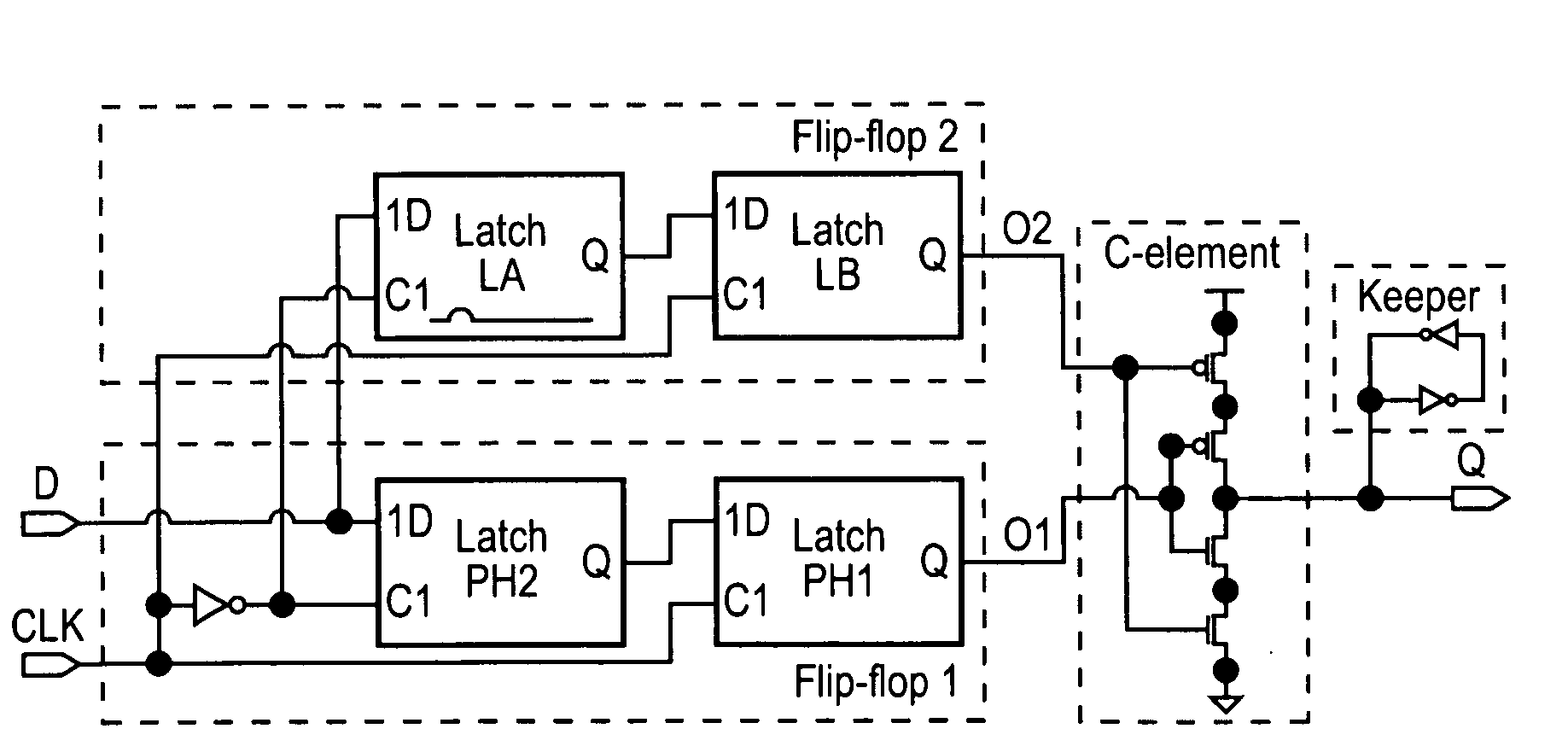
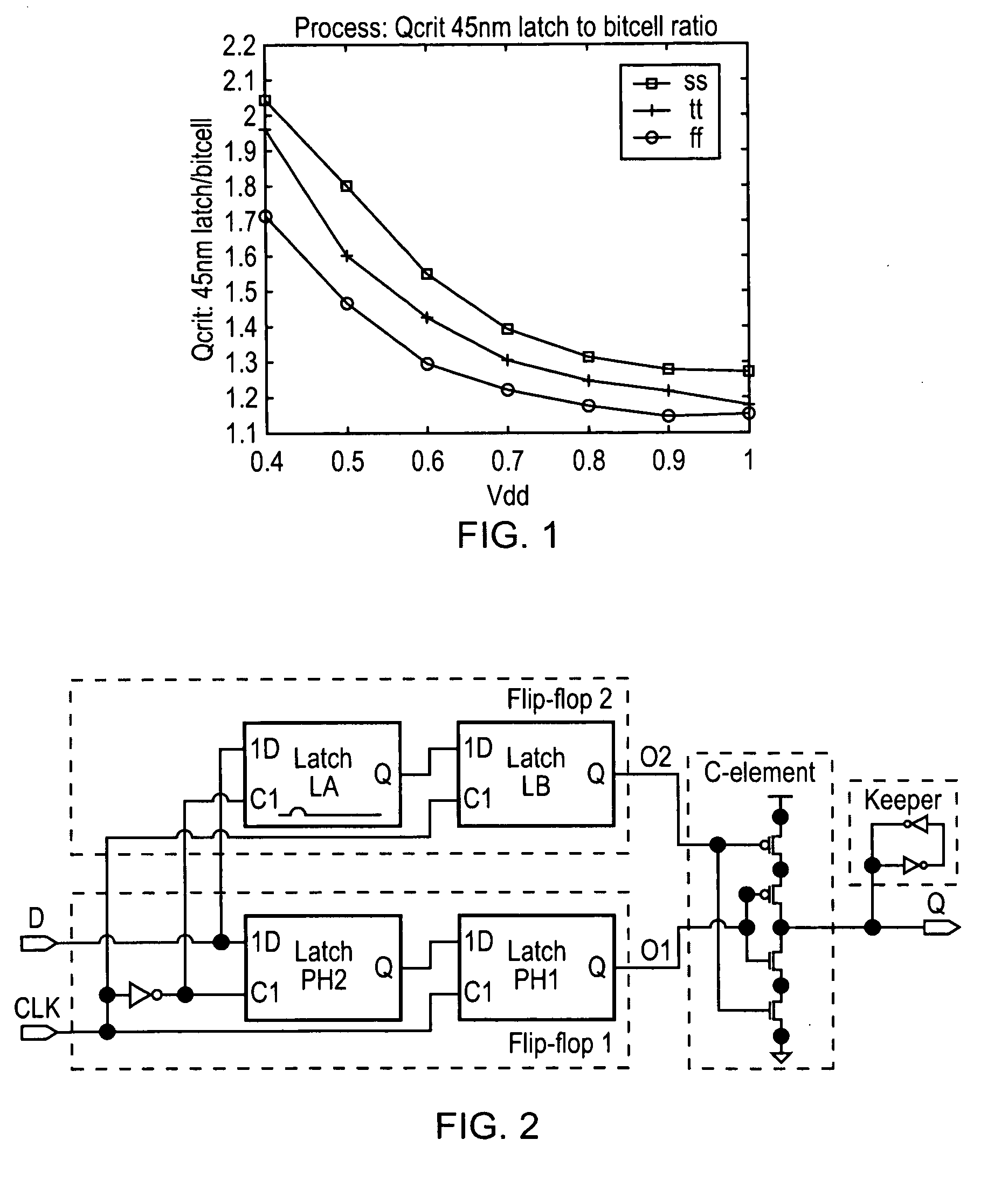
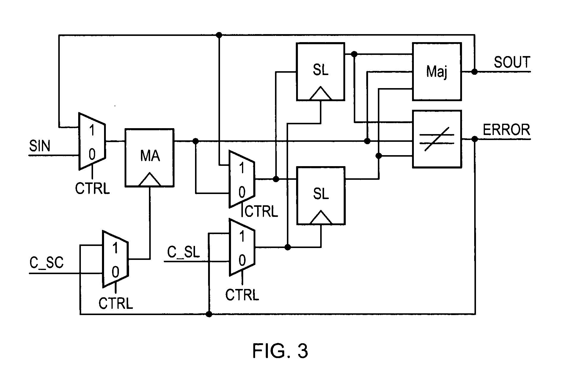
[0060]FIG. 4 shows an integrated circuit 2 including pipeline stages 4, 6 extending between sequential edge triggered storage circuit 8 which may be in the form of flip flops. Between the sequential storage circuits are respective incidences of combinatorial logic circuitry 10 which serve to receive signals from one or more preceding stages and to generate signals to be passed to one or more succeeding stages. The period of time between the capture of signal values by the sequential storage elements 8 for successive clock periods is the time that is available for the combinatorial logic circuitry 10 to evaluate its input so as to generate its output. Embodiments of the present invention provide a new design for the sequential storage circuit 8 which can detect and correct SEU's or soft errors occurring within the sequential storage circuit due to neutron or alpha particle strikes on the sequential storage circuit.

[0061]Integrated circuit 2 further comprises pulse generation circuit ...


PUM


Abstract

Sequential storage circuitry for an integrated circuit is disclosed that comprises storage circuitry comprising: a first storage element for storing, during a first phase of a clock signal, a first indication of an input data value received by said sequential storage circuitry; a second storage element coupled to an output of said first storage element, for storing a second indication of said input data value during a second phase of said clock signal; and error detection circuitry for detecting a single event upset error in any of said first and second storage elements comprising: two additional storage elements for storing third and fourth indications of said input data value respectively in response to a pulse signal derived from said clock signal; comparison circuitry for comparing said third and fourth indications of said input data value; and further comparison circuitry for comparing during a first phase of said clock signal said first indication and at least one of said third and fourth indications, and for comparing during a second phase of said clock signal said second indication and at least one of said third and fourth indications; and output circuitry for correcting any detected errors in said storage circuitry and for outputting an output value; said output circuitry being responsive to no match by said comparison circuitry to output said first indication during a first phase of said clock signal and said second indication during said second phase of said clock signal, and said output circuitry being responsive to a match by said comparison circuitry to output a value in dependence upon comparisons performed by said further comparison circuitry; said output circuitry being responsive to a match by said further comparison circuitry during a first phase of said clock signal to output said first indication during said first clock cycle and to a no match to output an inverted value of said first indication; and said output circuitry being responsive to a match by said further comparison circuitry during a second phase of said clock signal to output said second indication during said second phase of said clock signal and to a no match to output an inverted value of said second indication.

Description

BACKGROUND OF THE INVENTION[0001]1. Field of the Invention[0002]The field of the invention relates to the correction of soft errors or single event upset errors, such as those that arise from neutron or alpha particle strikes, within sequential storage circuitry of integrated circuits[0003]2. Description of the Prior Art[0004]A soft error or Single Event Upset Error (SEU) is a disturbance of a node within a circuit due to a hit on the silicon substrate by either high energy neutrons or alpha particles. Such a hit can produce a change of state or a transient voltage pulse at sensitive nodes in integrated circuits such as processors. Errors can occur due to SEU where it leads to a change in state in the state-holding elements that determine the architectural state of the integrated circuit, such as the RAM arrays, the register file, the architectural-state registers of a processor, or the flip-flops and latches within control logic. In the context of this document we consider an error...

Claims


Application Information

Patent Timeline
IPC IPC(8): G06F11/00
CPCH03K19/00392G06F11/183
Inventor CHANDRA, VIKAS
Owner ARM LTD
Why Eureka
Try Eureka