Method of manufacturing chip capacitor including ceramic/polymer composite

Active Publication Date: 2010-04-01
SAMSUNG ELECTRO MECHANICS CO LTD
View PDF6 Cites 9 Cited by
  • Summary
  • Abstract
  • Description
  • Claims
  • Application Information

AI Technical Summary

Benefits of technology

[0010]An aspect of the present invention provides a method of manufacturing a chip capacitor that can simplify the process, reduce manufacturing costs, replace existing MLCCs formed of a ceramic material, and have a low-loss value.

Problems solved by technology

Therefore, it becomes difficult to determine an appropriate dielectric composition.

Method used


Image

  • Method of manufacturing chip capacitor including ceramic/polymer composite
  • Method of manufacturing chip capacitor including ceramic/polymer composite
  • Method of manufacturing chip capacitor including ceramic/polymer composite

Examples


Embodiment Construction

[0026]Exemplary embodiments of the present invention will now be described in detail with reference to the accompanying drawings.

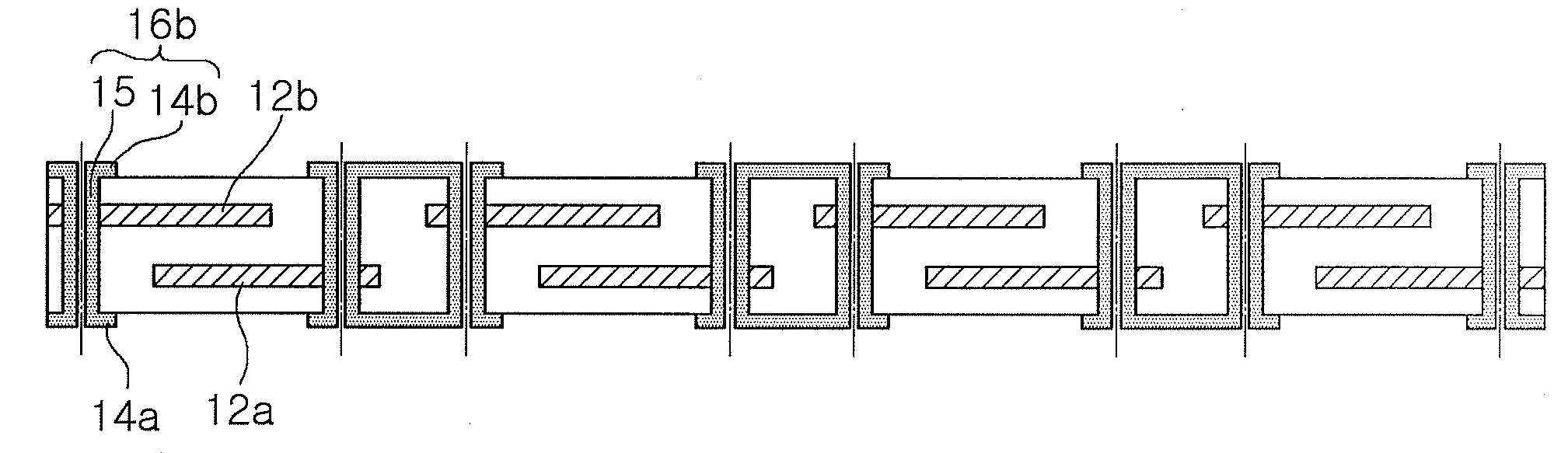
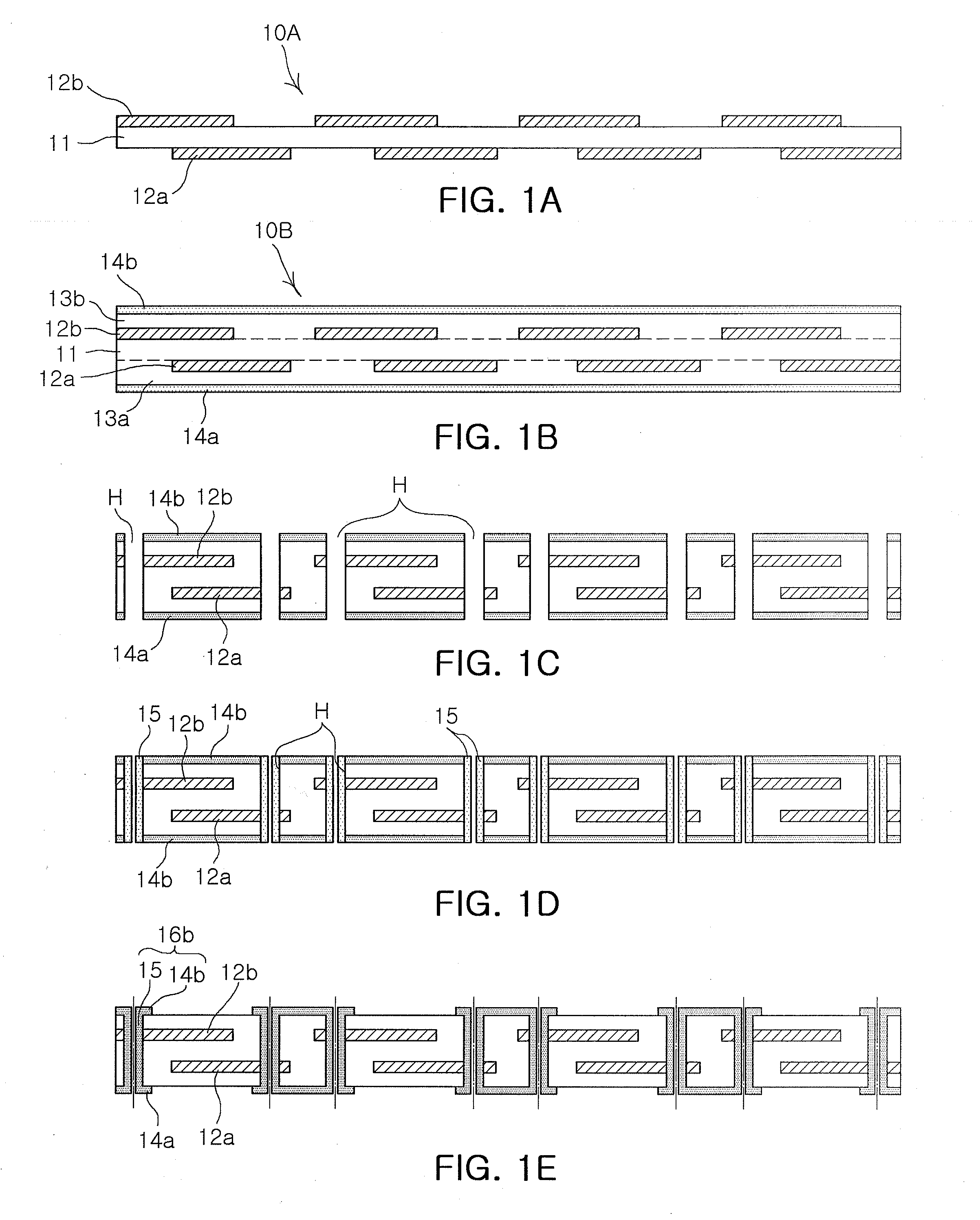
[0027]FIGS. 1A through 1E are cross-sectional views illustrating the process flow of a method of manufacturing a chip capacitor according to an exemplary embodiment of the invention.

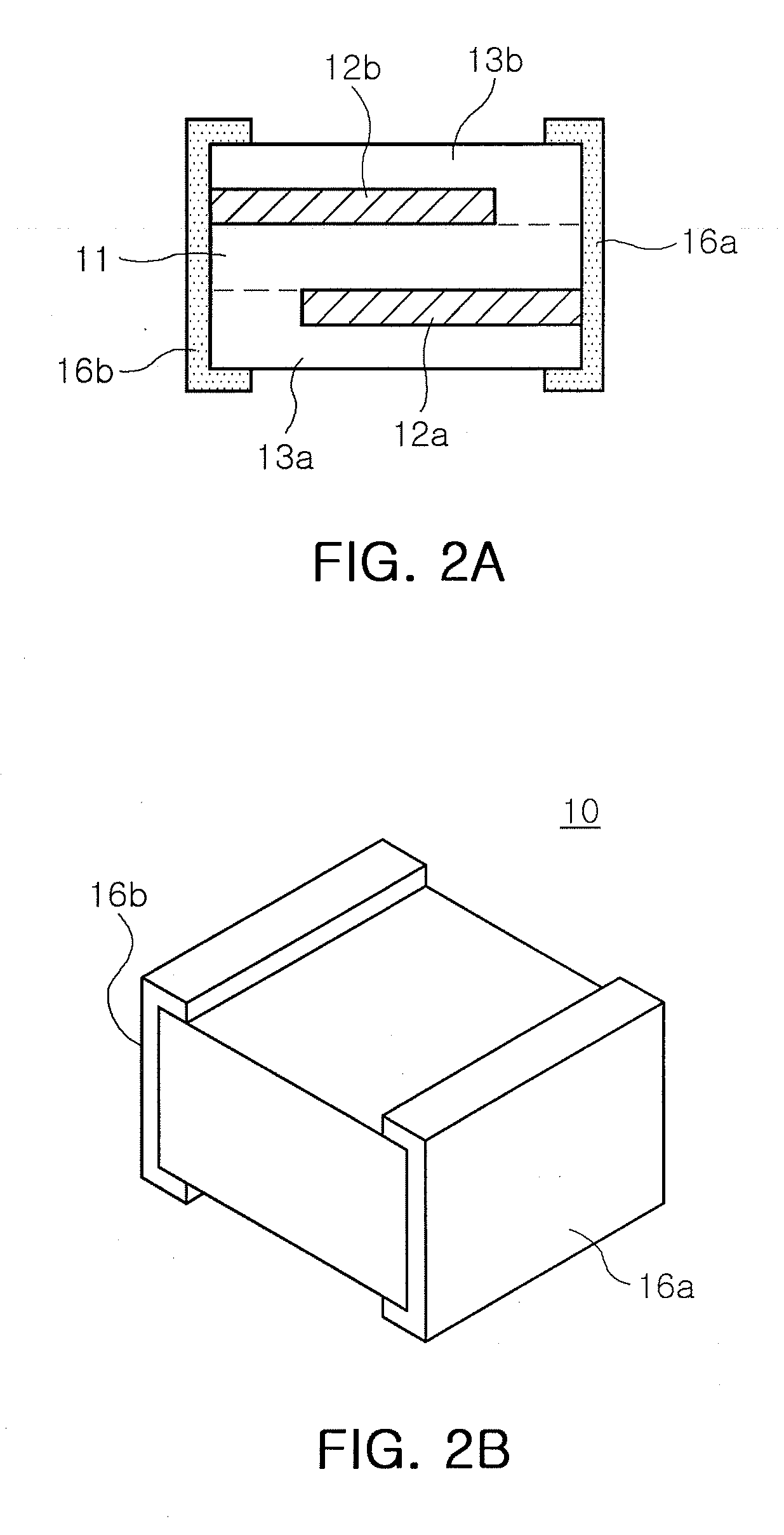
[0028]As shown in FIG. 1A, a capacitor lamination 10A is prepared. The capacitor lamination 10A has a dielectric sheet 11 and first and second internal electrodes 12a and 12b that are formed on both sides of the dielectric sheet 11 at predetermined intervals.

[0029]The dielectric sheet 11, which is used in this embodiment of the invention, is formed of a composite having ceramic powder and a polymer mixed together. The ceramic / polymer composite has a relatively low dielectric constant. However, since a high-frequency capacitor does not require a high dielectric constant, the ceramic / polymer composite can be advantageously used as long as it satisfies loss characteristics.

[0030]P...


PUM

PropertyMeasurementUnit
Fractionaaaaaaaaaa
Fractionaaaaaaaaaa
Timeaaaaaaaaaa

Abstract

A method of manufacturing a chip capacitor according to an aspect of the invention may include: preparing a capacitor lamination including a dielectric sheet formed of a composite having ceramic powder and a polymer mixed with each other, and first and second internal electrodes formed on both surfaces of the dielectric sheet at predetermined intervals; forming covering layers formed of an insulating material on both surfaces of the capacitor lamination; forming at least one first opening and at least one second opening in the capacitor lamination having the covering layers formed thereon to expose the first and second internal electrodes, respectively; forming plating layers in the first and second openings, the plating layers connected to the first and second internal electrodes; and dicing the result into chips on the basis of the first and second openings so that the plating layers formed in the first and second openings are provided as first and second external terminals.

Description

CROSS-REFERENCE TO RELATED APPLICATIONS[0001]This application claims the priority of Korean Patent Application No. 2008-0094859 filed on Sep. 26, 2008, in the Korean Intellectual Property Office, the disclosure of which is incorporated herein by reference.BACKGROUND OF THE INVENTION[0002]1. Field of the Invention[0003]The present invention relates to chip capacitors, and more particularly, to a method of manufacturing a high-frequency chip capacitor having a dielectric sheet formed of a ceramic / polymer composite.[0004]2. Description of the Related Art[0005]In general, as the speed and capacity of electronic apparatuses have increased, the frequency of signals transmitted along the lines of printed circuit boards has correspondingly increased. In order to transmit high-frequency signals without causing transmission loss, such as reflection loss, impedance matching between input and output terminals is of the utmost importance.[0006]As an operating frequency increases to a high freque...

Claims


Application Information

Patent Timeline
IPC IPC(8): H01G4/002H01G4/20H01G4/252H01G4/30H01G13/00
CPCH01G2/065H01G13/00Y10T29/49165Y10T29/417Y10T29/435H01G4/12H01G4/30
Inventor KIM, JIN CHEOLOH, JUN ROK
Owner SAMSUNG ELECTRO MECHANICS CO LTD
Why Eureka
Try Eureka