GaN-BASED SEMICONDUCTOR ELEMENT
a semiconductor element and gan technology, applied in the field of gan-based semiconductor elements, can solve the problems that the elements cannot help but be consequently broken down, and achieve the effects of reducing the leakage current flowing through the substrate, reducing current collapse, and high withstanding voltag
- Summary
- Abstract
- Description
- Claims
- Application Information
AI Technical Summary
Benefits of technology
Problems solved by technology
Method used
Image

Examples
first embodiment
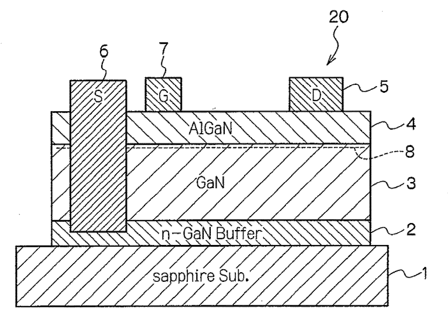
[0032]A GaN-based semiconductor element 20 according to the first embodiment of the present invention will be described in detail below, based on FIG. 1.
[0033]The GaN-based semiconductor element 20 is to be a GaN-based high electron mobility transistor (HEMT) as a GaN-based heterojunction field effect transistor (FET).
[0034]Such the GaN-based semiconductor element 20 comprises a buffer layer 2 formed on a sapphire (0001) substrate 1, a channel layer (an electron transport layer) 3 comprised of a undoped GaN layer on the buffer layer 2, and an electron supply layer 4 comprised of a undoped AlGaN layer formed on the channel layer 3. Moreover, the GaN-based semiconductor element 20 comprises a gate electrode (G) 7, a source electrode (S) 6 and a drain electrode (D) 5 formed on the electron supply layer 4 respectively.
[0035]In such the GaN-based semiconductor element 20, a two-dimensional electron gas 8 is generated at an interface between the channel layer 3 and the electron supply lay...
second embodiment
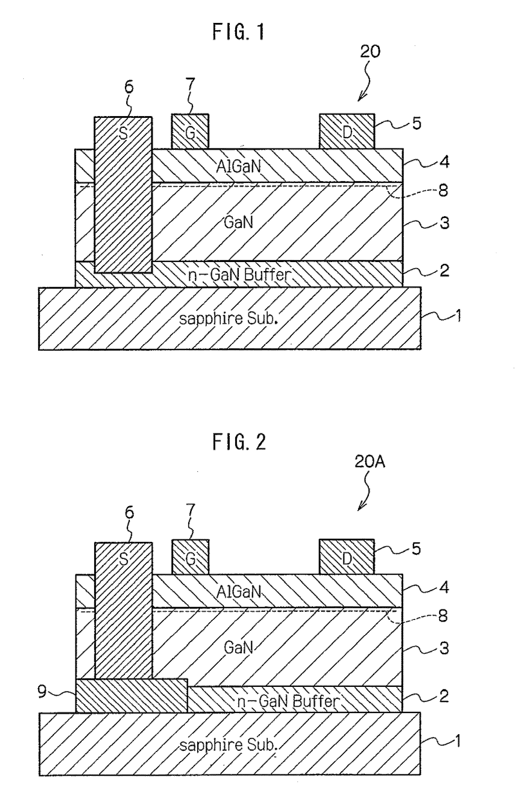
[0053]Next, a GaN-based semiconductor element 20A according to the second embodiment of the present invention will be described in detail below, based on FIG. 2.
[0054]An aspect of such the GaN-based semiconductor element 20A is that the following structure is to be adopted as a structure to be able to control an electric potential of a buffer layer 2 comprised of an n-GaN layer.
[0055]That is to say, in the structure to be able to control the electric potential of the buffer layer 2, there is provided a metal layer 9, which is selectively formed at a part except a region for forming the buffer layer 2 on a sapphire (0001) substrate 1, and which is ohmic contacted to the buffer layer 2. Moreover, the structure includes a configuration that a source electrode 6 is implanted into epitaxial layers (a channel layer 3 and an electron supply layer 4) formed on the buffer layer 2 and the metal layer 9, and that the source electrode 6 is extended to a depth reaching the metal layer 9 for elec...
third embodiment
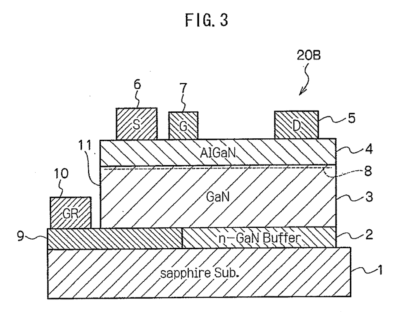
[0065]Next, a GaN-based semiconductor element 20B according to the third embodiment of the present invention will be described in detail below, based on FIG. 3.
[0066]An aspect of such the GaN-based semiconductor element 20B is that the following structure is to be adopted as a structure to be able to control an electric potential of a buffer layer 2 comprised of an n-GaN layer.
[0067]That is to say, in the structure to be able to control the electric potential of the buffer layer 2, there is provided a metal layer 9, which is selectively formed on a part except a region for forming the buffer layer 2 on a sapphire (0001) substrate 1, and which is ohmic contacted to the buffer layer 2. Moreover, the structure includes a configuration that a mesa structure 11 is formed at a part of epitaxial layers (a channel layer 3 and an electron supply layer 4) formed on the buffer layer 2 to be deep for reaching the metal layer 9, and that an electrode 10 is formed on a part of a top surface of th...
PUM
 Abstract
Description
Claims
Application Information
 - R&D
- Intellectual Property
- Life Sciences
- Materials
- Tech Scout
- Unparalleled Data Quality
- Higher Quality Content
- 60% Fewer Hallucinations
Browse by: Latest US Patents, China's latest patents, Technical Efficacy Thesaurus, Application Domain, Technology Topic, Popular Technical Reports.
© 2025 PatSnap. All rights reserved.Legal|Privacy policy|Modern Slavery Act Transparency Statement|Sitemap|About US| Contact US: help@patsnap.com