Method for dicing wafer and process for manufacturing liquid-discharging head using the dicing method
a technology of dicing wafers and liquid discharging heads, which is applied in the field of dicing wafers, can solve the problems of increasing the number of manufacturing steps
- Summary
- Abstract
- Description
- Claims
- Application Information
AI Technical Summary
Benefits of technology
Problems solved by technology
Method used
Image
Examples
first embodiment
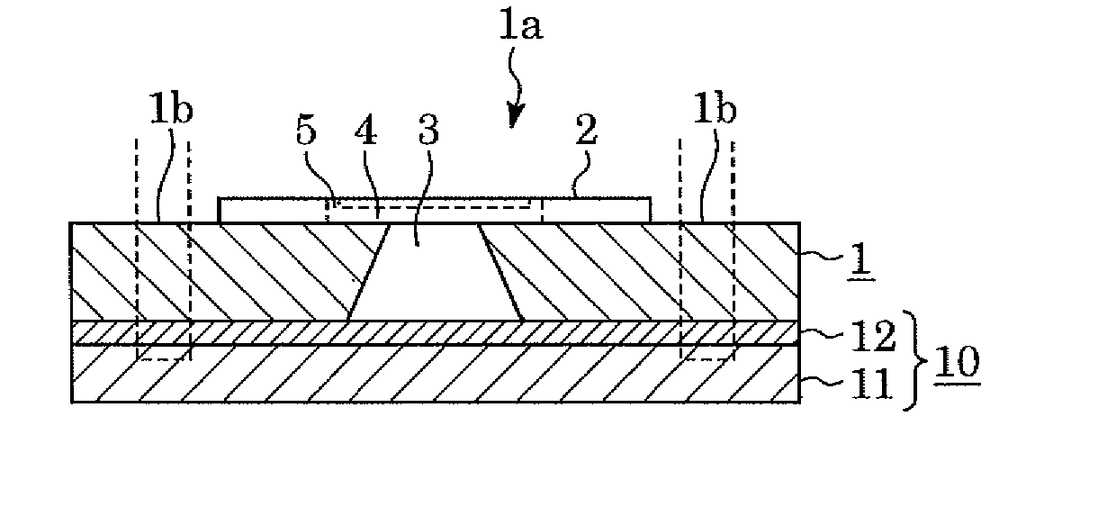
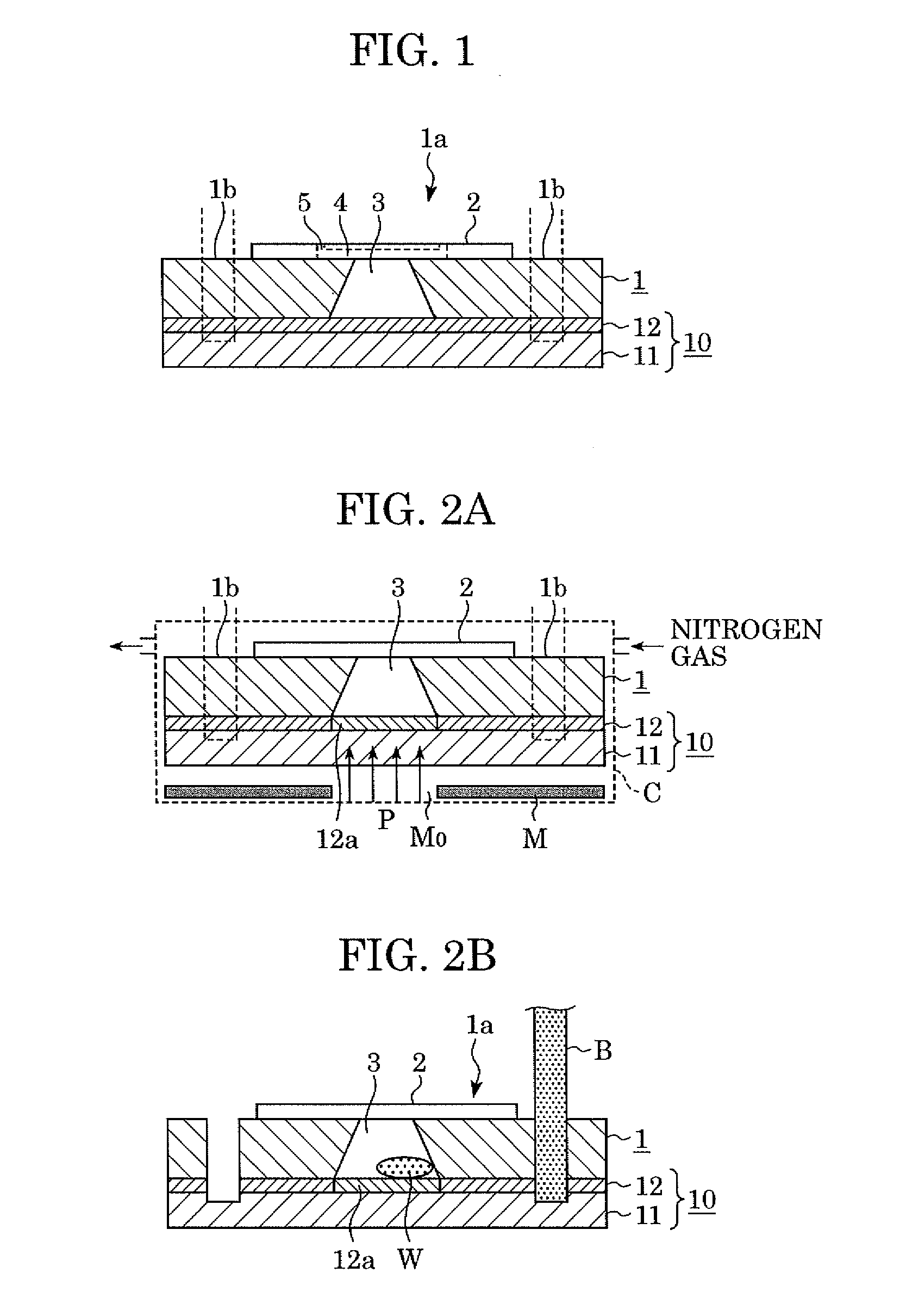
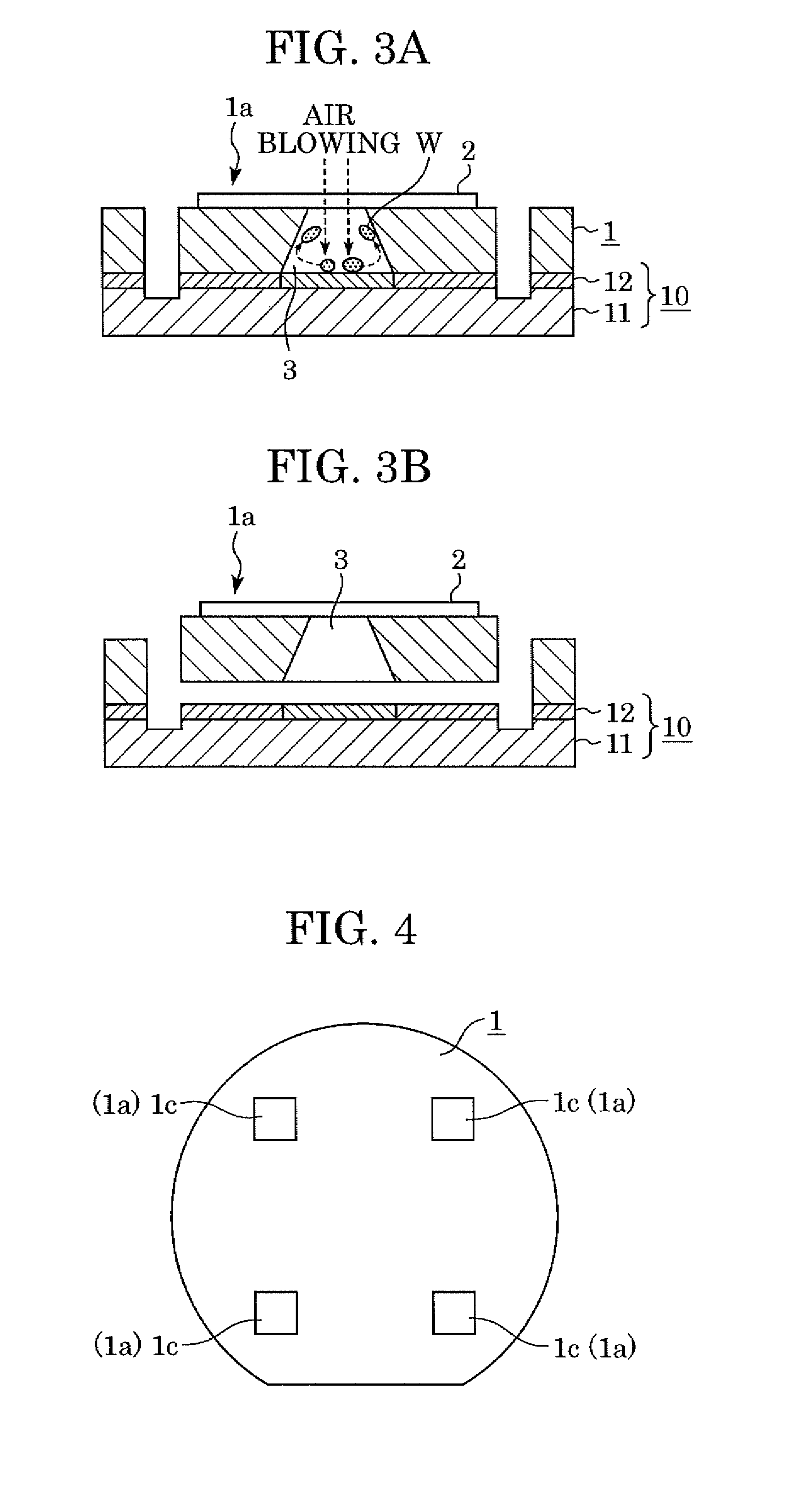
[0052]A first embodiment of the present invention provides a dicing method described below. With reference to FIG. 1, a wafer 1 to be diced has element sections 1a, which each include corresponding semiconductor circuit regions, nozzle layers 2 having orifices 5 and channels 4, and ink supply ports (liquid supply ports) 3. The semiconductor circuit regions and the nozzle layers 2 are arranged on the front face of the wafer 1 and form discharging devices. The liquid supply ports 3 extend from the rear face of the wafer 1 and communicate with the orifices 5 via the channels 4 placed therebetween. These components form element substrates for liquid-discharging heads. A dicing tape 10 including a bucking 11 and an adhesive 12 placed thereon is affixed to the rear face of the wafer 1. The element sections 1a are separated from each other by dicing the wafer 1 along dicing streets 1b extending along cutting lines. As shown in FIG. 2, before dicing is performed, ultraviolet light P is appl...
second embodiment
[0073]A second embodiment of the present invention will now be described with reference to FIGS. 9 to 13.
[0074]In the first embodiment, the wafer 1 is loosely fixed during dicing after the adhesive 12 is partly cured prior to dicing. Therefore, minimum regions of the adhesive 12 are selectively cured. However, the width of the adhesive layers 12a that are formed by curing regions of the adhesive 12 as described above before dicing is performed increases with an increase in the dose (irradiation dose) of ultraviolet light; hence, the cured regions are apt to have a width greater than a required value. This phenomenon is referred to as an increase in pattern size and caused by the scattering of a portion of ultraviolet light incident on the backing 11. In general, in order to prevent an adhesive of a dicing tape from remaining on separated elements during the pick up of the elements, the adhesive has a thickness less than that of a backing. Therefore, ultraviolet light is mostly scatt...
third embodiment
[0097]In the second embodiment, in order to prevent problems due to adhesive pieces derived from the dicing tape 10 from occurring, regions of the adhesive 12 that are exposed in the liquid supply ports 3 are cured and therefore reduced in adhesive strength before dicing is performed, whereby adhesive particles are created from the regions. Furthermore, it is necessary to prevent chippings from being created from portions of the adhesive 12 that correspond to the dicing streets 1b extending along cutting lines along which the wafer 1 is diced. In order to prevent such adhesive chippings from being created from the adhesive 12 subjected to dicing using a blade, the portions of the adhesive 12, which is included in the dicing tape 10, are cured before dicing is performed.
[0098]There are problems described below when the following regions and portions are simultaneously cured and therefore reduced in adhesive strength: the regions of the adhesive 12 that are exposed in the liquid suppl...
PUM
| Property | Measurement | Unit |
|---|---|---|
| angle | aaaaa | aaaaa |
| pitch | aaaaa | aaaaa |
| width | aaaaa | aaaaa |
Abstract
Description
Claims
Application Information
 - R&D
- Intellectual Property
- Life Sciences
- Materials
- Tech Scout
- Unparalleled Data Quality
- Higher Quality Content
- 60% Fewer Hallucinations
Browse by: Latest US Patents, China's latest patents, Technical Efficacy Thesaurus, Application Domain, Technology Topic, Popular Technical Reports.
© 2025 PatSnap. All rights reserved.Legal|Privacy policy|Modern Slavery Act Transparency Statement|Sitemap|About US| Contact US: help@patsnap.com


