
Warpage correction material and method for manufacturing fan out-type wafer level package

A wafer-level packaging and manufacturing method technology, applied in electrical components, electrical solid-state devices, circuits, etc., can solve problems such as warpage and deformation of circuit surfaces, and achieve the effect of reducing warpage and high quality reliability.

Pending Publication Date: 2019-11-12
TAIYO INK MFG
View PDF7 Cites 2 Cited by
  • Summary
  • Abstract
  • Description
  • Claims
  • Application Information

AI Technical Summary

Problems solved by technology

In addition, on the surface opposite to the rewiring layer and the lead frame, due to the shrinkage of the sealed sealing material during curing, warping deformation occurs in which the circuit surface protrudes.

Method used


Image

  • Warpage correction material and method for manufacturing fan out-type wafer level package
  • Warpage correction material and method for manufacturing fan out-type wafer level package
  • Warpage correction material and method for manufacturing fan out-type wafer level package

Examples


Embodiment

[0117] Next, the present invention will be described in more detail by giving examples, but the present invention is not limited to these examples.

[0118]

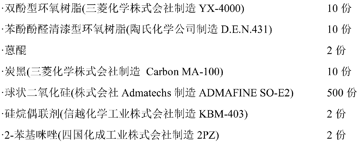
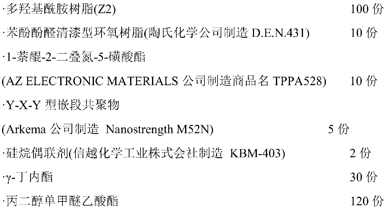
[0119] 100nm SiO formed on one side by Canosis Co., Ltd. 2 A 4-inch P-type silicon wafer with a thickness of 150 μm was diced with a dicing device to obtain semiconductor chips of 10 mm×10 mm square. Place a temporary fixing film on a flat substrate made of SUS, according to SiO 2 5 x 5 semiconductor chips were arranged vertically and horizontally in such a manner that the surface was in contact with the temporary fixing film and the semiconductor chips were spaced at 10 mm intervals in the vertical and horizontal directions. A 100 mm x 100 mm square sheet-shaped sealing material for semiconductors was laminated thereon so that the center positions were substantially aligned, and extrusion molding was performed at 150° C. for 1 hour using a heating press. As the encapsulant for semiconductors, the following material ...


PUM

PropertyMeasurementUnit
Thicknessaaaaaaaaaa
Epoxy equivalentaaaaaaaaaa
Acid valueaaaaaaaaaa

Abstract

Provided is a warpage correction material which can adjust the amount of warpage even at the temperature at which a fan out-type wafer level package (FO-WLP) is mounted, and at room temperature at which, for example, wafer transportation is performed, and thereby reduce the warpage of the WLP. This warpage correction material for a fan out-type wafer level package is characterized by comprising acurable resin composition including a component that is curable by means of an active energy ray and heat, wherein when the warpage correction material is formed into a flat film-shaped cured productby curing the warpage correction material by means of the active energy ray and heat, and the linear expansion coefficient alpha (ppm / DEG C) at 25 DEG C, the elastic modulus beta (GPa) at 25 DEG C, and the thickness gamma ([mu]m) of the cured product satisfy the following relational expression: 2000<=alpha*beta*gamma<=10000.

Description

technical field [0001] The present invention relates to a fan-out type warpage correction material for wafer level packaging in which an arrangement area of ​​electrodes for external connection is larger than the planar size of a semiconductor. Background technique [0002] In recent years, the demand for miniaturization in the field of semiconductor circuits and the like has gradually increased. To meet this demand, semiconductor circuits may be mounted in packages (Chip Size Packages) close to their chip size. As one of means for realizing chip-scale packaging, a packaging method called wafer-level packaging (Wafer Level Package, hereinafter sometimes abbreviated as WLP) in which wafer-level bonding and fragmentation are performed has been proposed. WLP has attracted attention because it can contribute to cost reduction and miniaturization. The WLP is flip-chip mounted on a circuit substrate on which electrodes are formed. [0003] In addition, along with miniaturization...

Claims


Application Information

Patent Timeline
IPC IPC(8): H01L23/12C08G59/62H01L23/00H01L23/29H01L23/31
CPCH01L23/29H01L23/562H01L23/31H01L23/12C08G59/62
Inventor 伊藤秀之佐藤和也荒井康昭
Owner TAIYO INK MFG
Learn More