Device and method for biasing a transistor amplifier

a transistor amplifier and device technology, applied in the field of devices and methods for biasing transistor amplifiers, can solve the problems of difficult to provide a high impedance value in an area-efficient manner, limited noise bandwidth, and not always available or practical, and achieve the effect of facilitating subdivision of reference current ir

Inactive Publication Date: 2009-07-23
KONTEL DATA SYST
View PDF5 Cites 5 Cited by
  • Summary
  • Abstract
  • Description
  • Claims
  • Application Information

AI Technical Summary

Benefits of technology

[0043]It would be appreciated by a person skilled in the art that at least one advantage of the present invention is in providing a biasing circuit for an amplifier which simultaneously provides a high impedance to ground, a variable biasing voltage, and a low-pass filter which assists in filtering out noise from the bias voltage applied to the amplifier input. This may be particularly advantageous in the context of MEMS technology where spatial limitations on integrated circuit chips must be taken into consideration and it is impractical to fabricate separate circuits dedicated to providing each of the above functions.
[0044]In a fifth broad form, the present invention provides circuitry for biasing a transistor amplifier with a DC-voltage signal, the transistor amplifier having a first input terminal, a second input terminal, and an output terminal coupled to the second input terminal, wherein said circuitry comprises:
[0046]an impedance transistor arranged in parallel with said capacitor, the transistor and capacitor forming a low-pass filter; and
[0047]a biasing circuit configured to controllably vary the DC-voltage signal for operatively biasing the amplifier, the biasing circuit including a cascaded current arrangement configured to subdivide a reference current into smaller currents for selectively generating voltage potentials for biasing the impedance transistor to adjustably filter a noise component of the DC-voltage signal via the low-pass filter before the DC-voltage signal is provided to the first input terminal.
[0048]Typically, the cascaded current arrangement includes a number of transistor cells to facilitate subdivision of a reference current IREF by m number of stages to IREF / NM−1.

Problems solved by technology

Accordingly, because the magnitude of the capacitor (C) is limited by the transducer's design, the bandwidth of the noise is limited by increasing the magnitude of the impedance (typically in the tens of Giga-Ohms).
However, where the biasing network is to be implemented on an integrated circuit, it is extremely difficult to provide a high impedance value in an area-efficient manner.
A large conventional impedance value typically requires a relatively large area an integrated circuit layout, which may not always be available or practical.

Method used


Image

  • Device and method for biasing a transistor amplifier
  • Device and method for biasing a transistor amplifier
  • Device and method for biasing a transistor amplifier

Examples


first embodiment

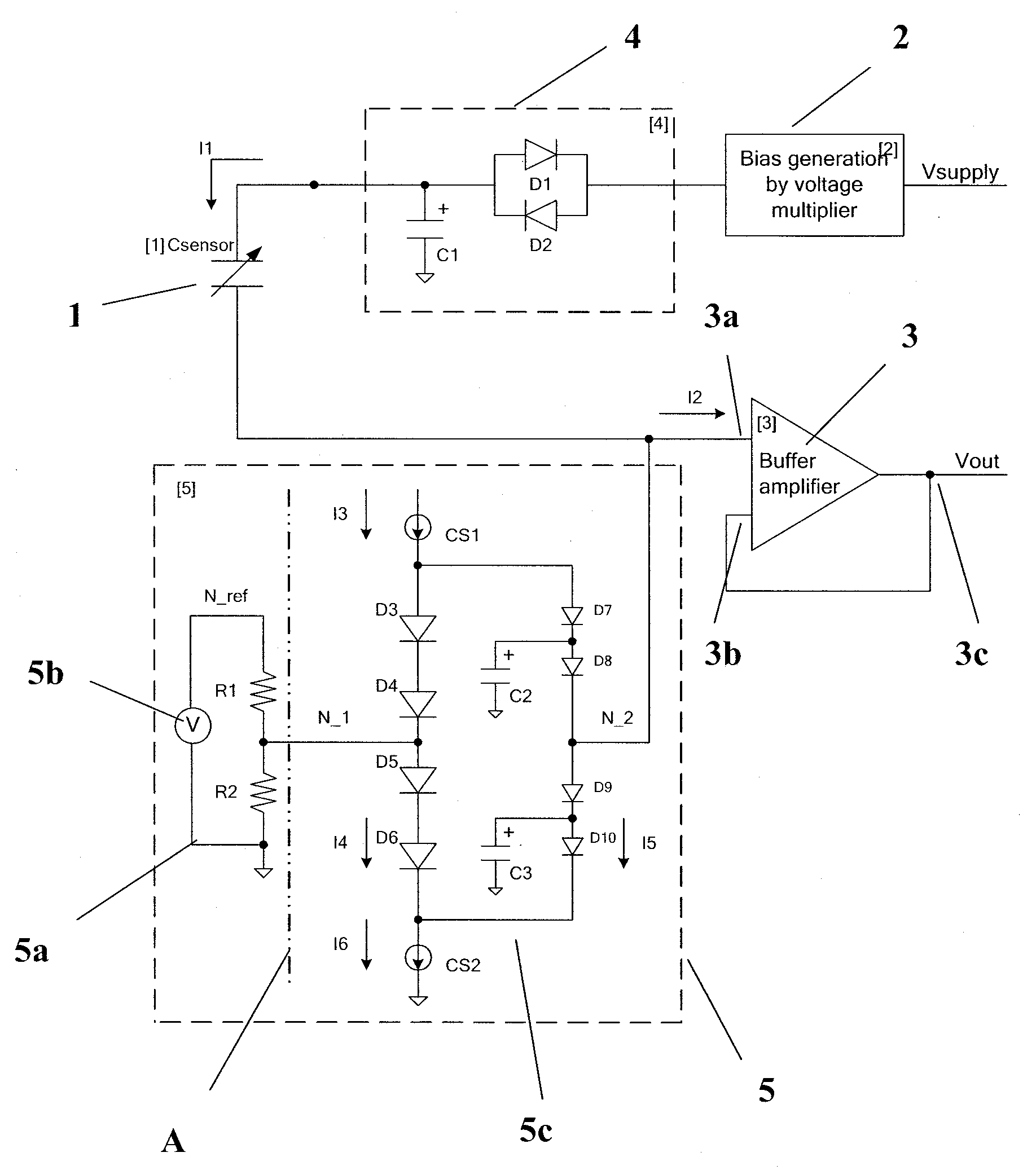
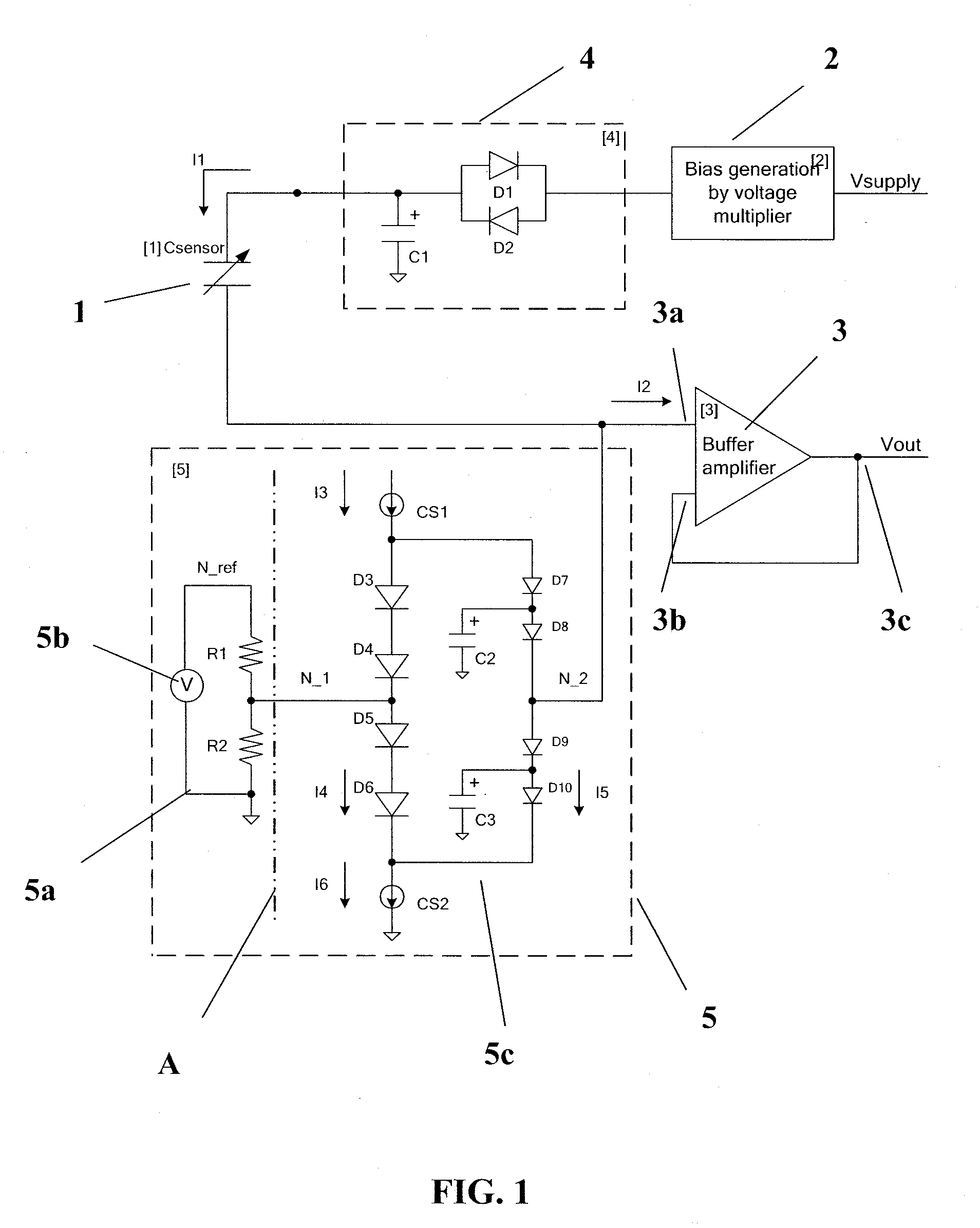
[0070]Referring firstly to FIG. 1, a device for use in biasing a transistor amplifier with a DC-voltage signal is shown operatively coupled to a buffer amplifier (3). The device and buffer amplifier (3) are typically fabricated on an integrated circuit.

[0071]In one embodiment, the buffer amplifier (3) is a FET amplifier having a first (positive) input terminal (3a), a second (negative) input terminal (3b) and an output terminal (3c). The output terminal (3c) is bootstrapped to the second input terminal (3b) via a feedback loop (not shown) to form a unity-gain or buffer amplifier.

[0072]A capacitive sensor (1) is operatively coupled to the first input terminal (3a) of the buffer amplifier (3). By way of example only, the capacitive sensor (1) can be part of an electret microphone. The capacitive sensor's (1) capacitance varies according to a received input signal—hereinafter referred to as Vsupply—which is to be transduced.

[0073]Vsupply is fed to the capacitive sensor (1) from a volta...

second embodiment

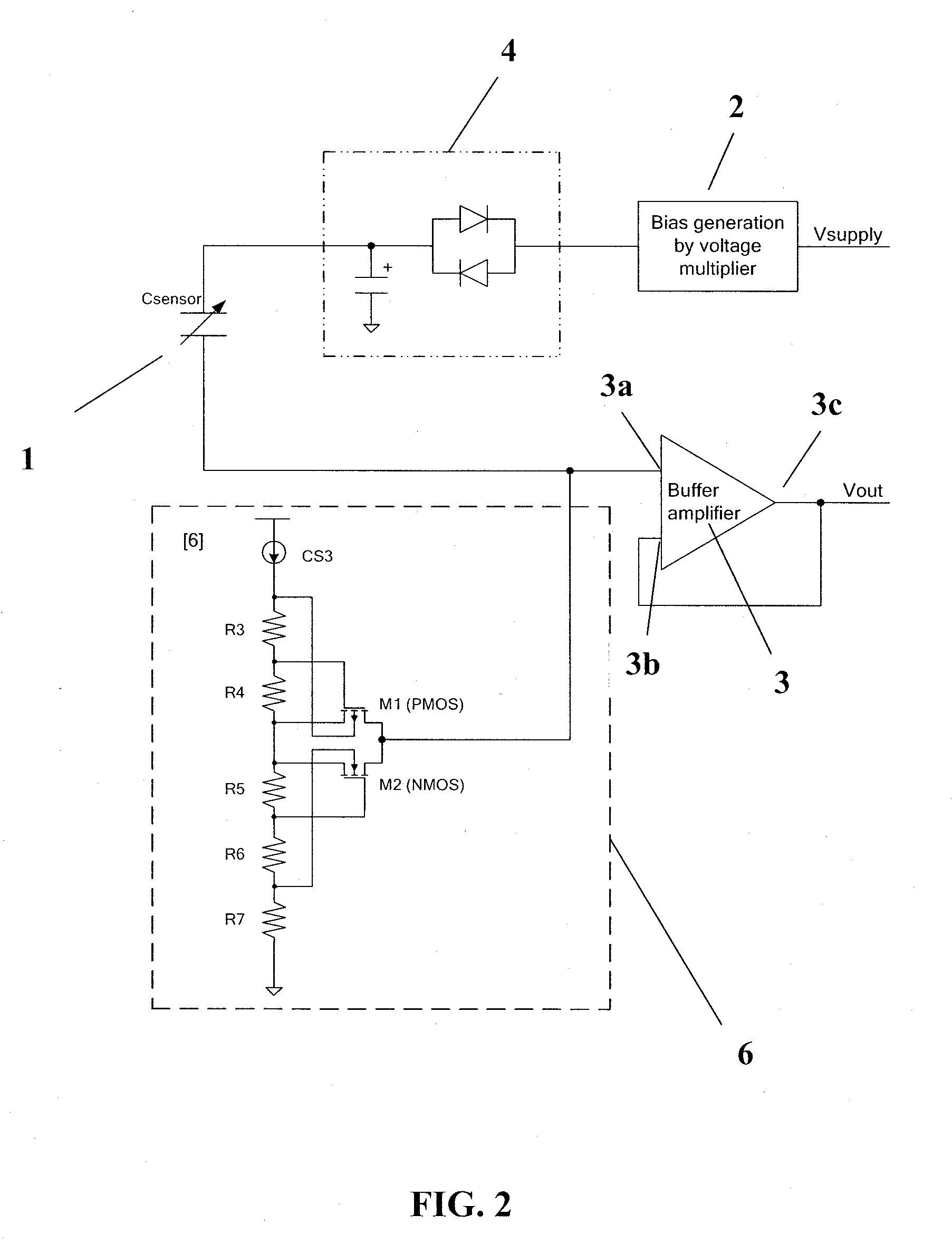
[0090]FIG. 2 of the drawings depicts a second embodiment device operatively coupled to a buffer amplifier (3).

[0091]It is a low pass network consisting of resistors (R3-R7), current source (CS3) and MOSFETs (M1, M2). Current source CS3 provides a bias current to resistors R3, R4, R5, R6 and R7 whereby a fixed voltage bias is able to be selected. As shown in FIG. 2, the configuration of M1, which is a PMOS device, and M2, which is an NMOS device, combines to act as very high value impedance elements. The conductivity of M1 and M2 is controlled by the respective gate voltages applied to M1 and M2 and determined by the sub-threshold properties of M1 and M2.

[0092]At an application level after the design is fabricated, the conductivity of M1 and M2 can be varied by trimming the resistor R4 and R5 or by connecting the gates of M1 and M2 to different potentials on the resistive ladder so as to alter an overdrive potential between gate-to-source of M1 and M2 respectively.

[0093]The low-pass ...


PUM


Abstract

Provided is circuitry for biasing a transistor amplifier with a DC-voltage signal, the transistor amplifier having a first input terminal, a second input terminal, and an output terminal coupled to the second input terminal. The circuitry includes a sensor capacitor connected to the first input terminal and an impedance transistor arranged in parallel with said capacitor, the transistor and capacitor forming a low-pass filter. The circuitry also includes a biasing circuit configured to controllably vary a DC-voltage signal for operatively biasing the amplifier, the biasing circuit including a cascaded current arrangement configured to subdivide a reference current into smaller currents for selectively generating voltage potentials for biasing the impedance transistor to adjustably filter a noise component of the DC-voltage signal via the low-pass filter before the DC-voltage signal is provided to the first input terminal.

Description

CROSS-REFERENCE TO RELATED APPLICATIONS[0001]This is a continuation-in-part of prior U.S. patent application Ser. No. 11 / 744,986, filed on Jul. 9, 2007, which is incorporated herein by reference in its entirety.TECHNICAL FIELD[0002]The present invention relates to an apparatus and method for biasing a transistor amplifier and in particular, FET transistor amplifiers which are fabricated on integrated circuit chips.BACKGROUND OF THE INVENTION[0003]Metal Oxide Semiconductor Field Effect Transistors (MOSFETs) and Junction Field Effect Transistors (JFETs) are often used as the building blocks of low-noise amplifier devices fabricated on integrated circuit chips. Such amplifiers are useful for instance in audio applications, capacitive sensor applications, and thermal sensor detection applications where it is important to minimise the adverse effects of noise arising from, amongst other things, a DC-voltage bias source, and electronic elements that comprise such DC-voltage biasing circui...

Claims


Application Information

Patent Timeline
Patent Type & Authority Applications(United States)
IPC IPC(8): H03F3/04H03H7/00
CPCH03F1/30H03F3/45475H03F2200/213H03H11/1291H03F2203/45244H03F2203/45622H03H7/0153H03F2203/45136H03H7/0107
Inventor LI, PING WAILI, CONG KEWANG, WEI
Owner KONTEL DATA SYST
Why Eureka
Try Eureka