
Securing Authenticity of Integrated Circuit Chip

a technology of integrated circuit chips and authenticity, applied in the field of lithographic equipment, can solve problems such as tampered final ic, ic's made in semiconductor foundries are vulnerable to tampering, and unexpected failures in the field use of ic's, so as to improve the trust level of ic and achieve greater customer interest and support

Active Publication Date: 2009-04-16
ASML HLDG NV
View PDF6 Cites 32 Cited by
  • Summary
  • Abstract
  • Description
  • Claims
  • Application Information

AI Technical Summary

Benefits of technology

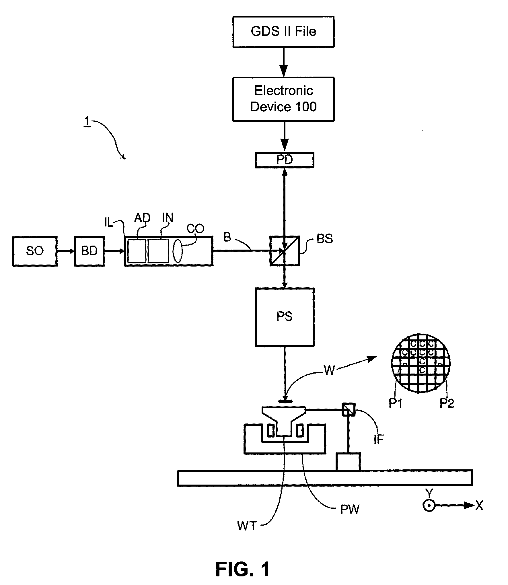
[0012]According to one embodiment of the invention, a process by which a lithography tool could be used to improve the level of trust in the IC even when made at an untrusted foundry is described. The lithography tool is used to print unique codes directly into the silicon which can later be read non-destructively to verify the chip origin and design. This can be done with mask based or maskless lithography tools. By embedding the security process within the maskless tool software and architecture, the process becomes tamper-proof. As such, secure printing approaches may offer the needed impetus to gain greater customer interest and support for maskless technology.

Problems solved by technology

IC's made in semiconductor foundries are vulnerable to tampering.
Tampering can result in unexpected failures in the field use of IC's, which is unacceptable particularly in critical areas such as medical electronics and / or military applications.
In an untrusted foundry, lack of control could result in a substitute GDS file or mask to be inserted into the process, thereby leading to a tampered with final IC.
Sufficient controls to guard against intrusive patterns, counterfeit copies of IC designs, or unwanted alterations may not be in place at all foundries.
The burdens required to insist on stricter controls on protocol are likely cost prohibitive.
With these conventional testing standards there may not be assurety if each and every IC will be authentic.
Further, these methods are inherently destructive by nature leading to the test IC becoming unusable after the test is carried out with no 100% guarantee that any other IC in the lot will be authentic.
In other words, trust cannot be added to ICs after fabrication and mere electrical testing and / or reverse engineering cannot be relied upon to detect undesired alterations in ICs on an IC-by-IC basis.
By embedding the security process within the maskless tool software and architecture, the process becomes tamper-proof.
Alternatively, if there is a mismatch in the daughter code patterns, the IC is declared as defective or untrusted.

Method used


Image

  • Securing Authenticity of Integrated Circuit Chip
  • Securing Authenticity of Integrated Circuit Chip
  • Securing Authenticity of Integrated Circuit Chip

Examples


example embodiments

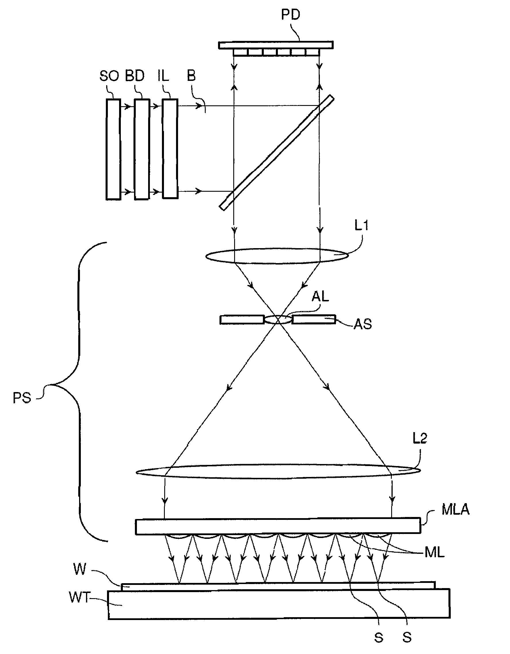
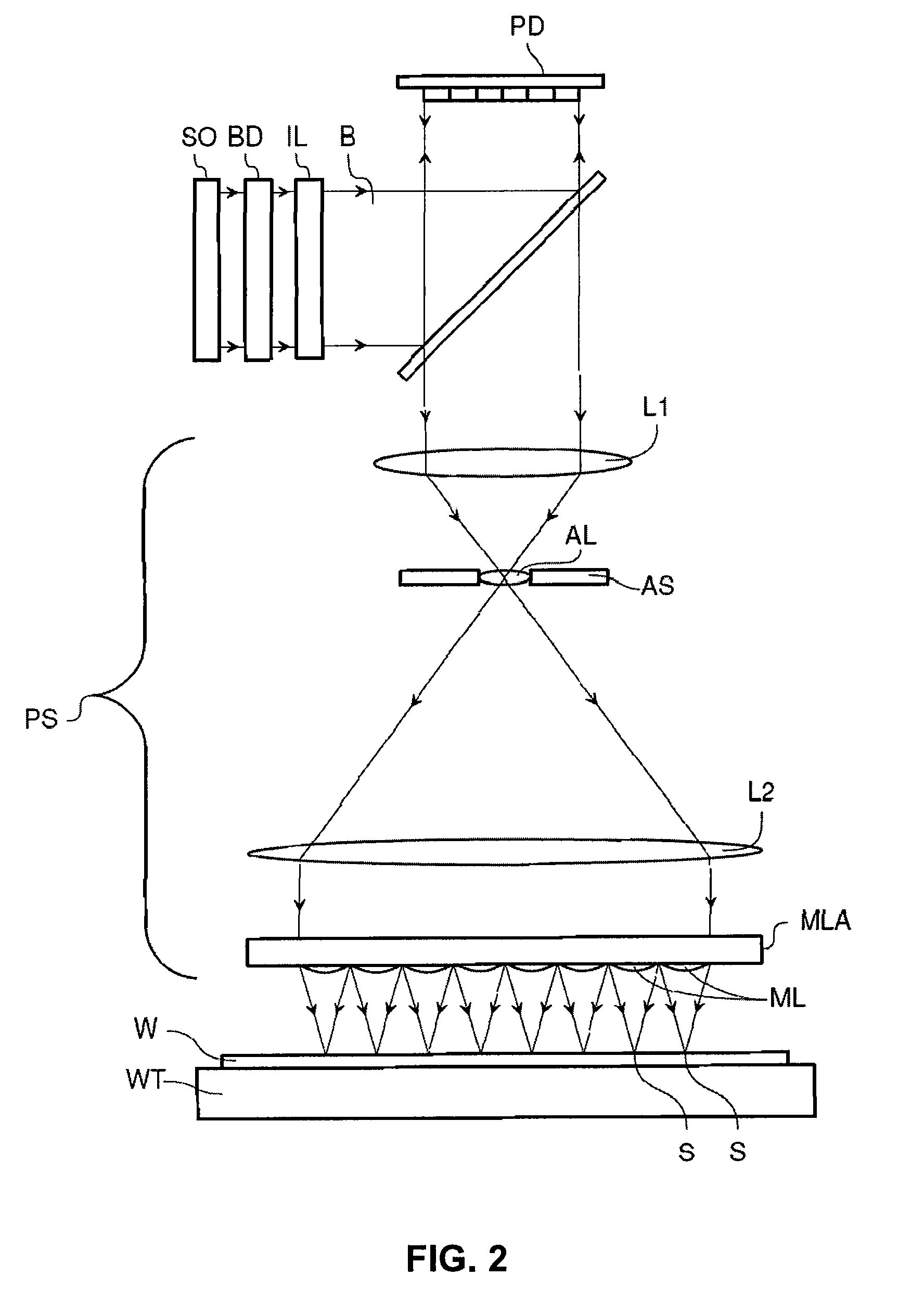
[0081]Generally, a system and method are provided for non-destructively testing an IC device manufactured at a foundry. For example, an integrated circuit chip may be securely fabricated at an untrusted foundry by later verifying authenticity of the integrated circuit chip based on a valid usage of an original source code file associated with a semiconductor manufacturing process of the integrated circuit chip. The integrated circuit chip may be authenticated by matching a first set of unique daughter codes generated during fabrication with a second set of unique daughter codes generated independently by some entity other than the foundry. In this way, a trusted electronics integrator may compare the first and second unique daughter codes to nondestructively determine whether the integrated circuit chip is a trusted device or a tampered device.

[0082]FIG. 4 depicts an exemplary general flowchart for transferring a set of daughter codes as pattern(s) onto one or more physical area(s) ...


PUM


Abstract

A system and method are provided for securely manufacturing a device at a foundry. For example, an integrated circuit chip may be securely fabricated at an untrusted foundry by later verifying authenticity of the integrated circuit chip based on a valid usage of an original source code file associated with a semiconductor manufacturing process of the integrated circuit chip. The integrated circuit chip may be authenticated by matching a first set of unique daughter codes generated during fabrication with a second set of unique daughter codes generated independently by some entity other than the foundry. In this way, a trusted electronics integrator may compare the first and second unique daughter codes to nondestructively determine whether the integrated circuit chip is a trusted device or a tampered device.

Description

CROSS REFERENCE TO RELATED APPLICATIONS[0001]This application claims priority under 35 U.S.C. §119(e) to U.S. Provisional Patent Application No. 60 / 980,341, filed Oct. 16, 2007, which is incorporated by reference herein in its entirety.BACKGROUND[0002]1. Field of the Invention[0003]The present invention generally relates to a lithographic apparatus and a system and method for non-destructive testing of trusted integrated circuits fabricated in an untrusted foundry to secure authenticity of the integrated circuits.[0004]2. Related Art[0005]A lithographic apparatus is a machine that applies a desired pattern onto a substrate or part of a substrate. A lithographic apparatus can be used, for example, in the manufacture of flat panel displays, integrated circuits (ICs) and other devices involving fine structures. Such a lithographic apparatus can be mask-based or maskless. In a conventional apparatus, a patterning device, which can be referred to as a mask or a reticle, can be used to ge...

Claims


Application Information

Patent Timeline
IPC IPC(8): G06F17/50G03B27/52
CPCG03B27/52G03F7/70541
Inventor IVALDI, JUAN C.
Owner ASML HLDG NV
Learn More