Semiconductor laser device and fabrication method for the same

a laser device and semiconductor technology, applied in semiconductor lasers, laser details, electrical devices, etc., can solve the problems of increasing the oscillation threshold current, affecting the stability of the active layer, and the shortage of electron-hole pairs, so as to reduce the external differential quantum efficiency and stable fundamental transverse mode oscillation. , the effect of small decreas

Active Publication Date: 2009-02-05
PANASONIC SEMICON SOLUTIONS CO LTD
View PDF7 Cites 7 Cited by
  • Summary
  • Abstract
  • Description
  • Claims
  • Application Information

AI Technical Summary

Benefits of technology

[0018]An object of the present invention is providing a semiconductor laser device that is small in decrease of the external differential quantum efficien...

Problems solved by technology

However, if the reflectance of the front end face is too low, the laser light fed back inside the cavity is reduced, causing increase in oscillation threshold current.
Also, with the reflectance of the front end face being low, when the semiconductor laser device is applied to an optical disk, noise is likely to occur due to return light reflected from the optical disk (return light-induced noise).
This is likely to cause shortage of electron-hole pairs in the active layer on the front end face side especially during high-output operation.
Such shortage of electron-hole pairs may become a cause of saturation of the luminous efficiency.
In attainment of a high-output laser having an output of 200 mW to 300 mW or more, this may degrade the temperature characteristic resulting in serious obstruction.
In this case, however, physical damage may be left behind on the ridge sidewalls, causing a leak at the interface between the ridge sidewalls and a current narrowing layer and thus deteriorating the current narrowing effect.
As a result, the light distribution i...

Method used


Image

  • Semiconductor laser device and fabrication method for the same
  • Semiconductor laser device and fabrication method for the same
  • Semiconductor laser device and fabrication method for the same

Examples


Embodiment Construction

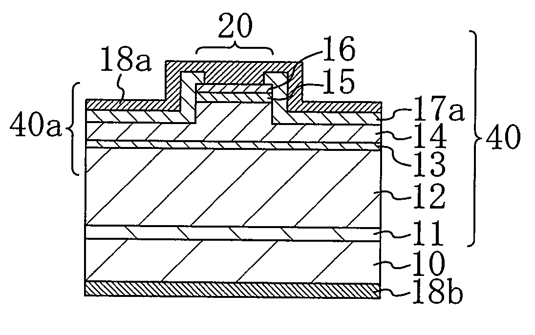
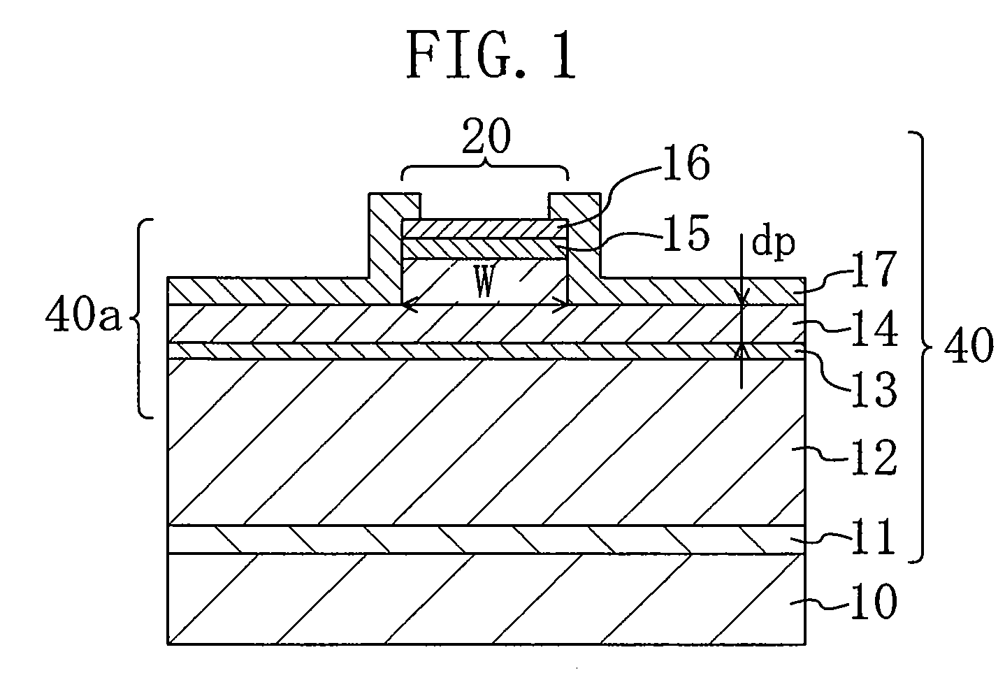
[0037]Hereinafter, an embodiment of the present invention will be described with reference to the accompanying drawings. FIG. 1 is a cross-sectional view of a semiconductor laser device of this embodiment, which shows the cross-sectional configuration in a portion thereof closer to the front end face from which laser light is extracted. As shown in FIG. 1, the semiconductor laser device of this embodiment is a red laser device including a cavity structure 40 formed on a substrate 10 made of n-type GaAs having a plane tilted from (100) plane by 10° in [011] direction as the principal plane. Note that a P electrode and an N electrode are omitted in FIG. 1.

[0038]On the substrate 10, formed sequentially are a buffer layer 11 made of n-type GaAs having a thickness of 0.5 μm, a first clad layer 12 made of n-type (Al0.7Ga0.3)0.51In0.49P having a thickness of 2 μm, an active layer 13, a second clad layer 14 made of p-type (Al0.7Ga0.3)0.51In0.49P, a protection layer 15 made of p-type Ga0.51I...


PUM


Abstract

The semiconductor laser device includes a cavity structure having a first clad layer, an active layer and a second clad layer formed on a substrate. The second clad layer has a stripe portion extending between the front end face from which laser light is extracted and the rear end face opposite to the front end face. The stripe portion has a first region located closer to the front end face, a second region located closer to the rear end face and a change region whose width changes located between the first and second regions. The effective refractive index difference between the inside and outside of the stripe portion in the change region is greater than that in the first region.

Description

CROSS-REFERENCE TO RELATED APPLICATIONS[0001]This application claims priority under 35 U.S.C. §119 on Patent Application No. 2007-197119 filed in Japan on Jul. 30, 2007, the entire contents of which are hereby incorporated by reference.BACKGROUND OF THE INVENTION[0002]1. Technical Field[0003]The present invention relates to a semiconductor laser device and a fabrication method for the same, and more particularly to red and infrared semiconductor laser devices and fabrication methods for the same[0004]2. Background Art[0005]In these days, demands for a light source for a high-speed writable optical disk system, such as a recording 16x DVD having not only playback function but also recording function, have increasingly grown. For such a light source, required is a semiconductor laser device having at least 300 mW high-output operation capability.[0006]In general, in high-output operation of a semiconductor laser device, the cavity end face from which laser light is extracted (front en...

Claims


Application Information

Patent Timeline
IPC IPC(8): H01S5/028
CPCB82Y20/00H01S5/0287H01S5/0655H01S5/1039H01S5/1064H01S5/34326H01S5/22H01S5/2214H01S5/2216H01S5/2218H01S5/162
Inventor TAKAYAMA, TORUSATO, TOMOYAKIDOGUCHI, ISAO
Owner PANASONIC SEMICON SOLUTIONS CO LTD
Why Eureka
Try Eureka