
Substrate processing method, substrate processing apparatus and recording medium

Inactive Publication Date: 2009-01-01
TOKYO ELECTRON LTD
View PDF5 Cites 15 Cited by
  • Summary
  • Abstract
  • Description
  • Claims
  • Application Information

AI Technical Summary

Benefits of technology

[0015]Accordingly, an object of the present invention, having been completed by addressing the issues discussed above, is to provide a substrate processing method and the like, which make it possible to release water in an insulating film with a low dielectric constant exposed at a recessed portion having been formed on a substrate through an etching process, disallow ready absorption of any additional water into the insulating film and remove an undesirable metal compound formed at a metal layer having become exposed at the recessed portion through the etching process or the like.
[0019]According to the present invention described above, the water present in the low dielectric constant insulating film can be released to a sufficient extent through the hydrogen radical processing and the low dielectric constant insulating film exposed at the recessed portion can be rendered hydrophobic through the hydrophobicity processing executed in direct succession following the hydrogen radical processing. As a result, the water content in the low dielectric constant insulating film can be reduced to a sufficient extent and also, any further absorption of water into the low dielectric constant insulating film is effectively prevented. This, in turn, improves the electrical characteristics and the mechanical strength of the low dielectric constant insulating film. The surface of the metal layer exposed at the recessed portion is cleaned through the hydrogen radical processing and thus, any undesirable metal compound that may have been formed during the etching process or the like at the exposed surface of the metal layer can be removed through the hydrogen radical processing. Consequently, any wiring metal embedded in the recessed portion can be connected to the metal layer with less resistance.
[0020]In addition, the hydrogen radical processing phase and the hydrophobicity processing phase are executed in succession in a low pressure environment without exposing the processing target substrate to air. Thus, even if the hydrogen radical processing renders the composition of the low dielectric constant insulating film exposed at the recessed portion to that which allows ready water absorption, reabsorption of water into the low dielectric constant insulating film prior to completion of the subsequent hydrophobicity processing can be effectively prevented.
[0022]Through the hydrophobicity processing phase, the low dielectric constant insulating film is rendered hydrophobic as a water-repellent layer is formed at the exposed surface of the low dielectric constant insulating film through a chemical reaction with the specific processing gas. The presence of such a water-repellent layer prevents reabsorption of water into the low dielectric constant insulating film. The specific gas used during this phase should be a silylating gas obtained from a compound that includes, for instance, a silazane (Si—N) bond within the molecules thereof. In such a case, a water-repellent layer will be formed as the exposed surface of the low dielectric constant insulating film having become damaged during the etching process or the like is silylated with the silylating gas. Namely, through the use of the silylating gas, a water-repellent layer is formed while restoring the quality of the low dielectric constant insulating film having been damaged during the etching process.
[0025]According to the present invention described above, the etching processing, the hydrogen radical processing and the hydrophobicity processing can be executed in succession without exposing the processing target substrate to air and thus, absorption of water into the low dielectric constant insulating film during the interval between the etching processing and the hydrogen radical processing as well as during the interval between the hydrogen radical processing and the hydrophobicity processing can be effectively prevented. In addition, since the hydrogen radical processing and the hydrophobicity processing are executed in succession after the low dielectric constant insulating film undergoes the etching processing, reabsorption of water into the low dielectric constant insulating film is effectively prevented once the water content in the film has been sufficiently lowered and any undesirable metal compound formed at the exposed surface of the metal layer during the etching process or the like can be eliminated.
[0026]According to the present invention, water present in the low dielectric constant insulating film exposed at the recessed portion formed by etching the substrate is first released to a sufficient extent, further absorption of water is inhibited and any undesirable metal compound formed at the metal layer having become exposed at the recessed portion through the etching processing or the like can be removed. As a result, the electrical resistance at the metal wiring can be kept to a low level, the low dielectric constant insulating film is allowed to sustain its low dielectric constant and a reduction in the mechanical strength of the low dielectric constant insulating film is prevented which, in turn, allows, a multilayer wiring structure with superior electrical characteristics and mechanical strength to be formed on the substrate.

Problems solved by technology

If copper is embedded to fill the wiring groove or the wiring hole to connect the horizontal copper wiring (wiring layer) with the vertical copper wiring with an undesirable copper compound film present at the surface of the copper wiring exposed at the bottom of the wiring groove or the wiring hole, the electrical resistance will increase over the connection area, giving rise to a concern that desirable electrical characteristics may not be achieved in the multilayer wiring structure.
While such a porous low-k material provides significant advantages when used as the interlayer insulating material, it absorbs water readily and thus gives rise to a concern that the moisture having penetrated the film may compromise both the electrical characteristics and the mechanical characteristics.
More specifically, if the low-k film contains moisture, the dielectric constant of the low-k film increases, resulting in an increase in the interlayer capacity in the multilayer wiring structure and a delay in electric signal transmission.
If moisture penetrates such a low-k film and reduces the mechanical strength of the film, a wiring groove or a wiring hole with a desired shape can no longer be formed with ease.
Furthermore, if the low-k film does not have sufficient mechanical strength, the film cannot retain its shape and thus, various types of films cannot be stacked on the low-k film.
As a result, a wiring structure with a greater number of players cannot be formed reliably.
Moreover, an interlayer dielectric film constituted of a material having a low dielectric constant such as a low-k film becomes readily damaged during an etching process or an ashing process (e.g., an ashing process executed by using oxygen plasma.
For this reason, as the interlayer dielectric film having undergone the etching process or the ashing process is taken out and exposed to air and moisture from the air is absorbed by the interlayer dielectric film, the electrical characteristics and the mechanical characteristics of the interlayer dielectric film may become significantly compromised.
However, while the technology disclosed in patent reference literature 1 prevents any additional water from becoming absorbed into the interlayer dielectric film by silylating the interlayer dielectric film having undergone the etching process and thus restoring it from any damage that may have occurred at the surface of the interlayer dielectric film during the etching process, the publication does not disclose effective measures for removing the water already present in the interlayer dielectric film to a sufficient extent.
Thus, there is bound to be a limit to how much the electrical characteristics and the mechanical strength of the interlayer dielectric film can be improved.
In addition, even when the side surfaces of the wiring groove or the wiring hole formed in the interlayer dielectric film are silylated, a metal compound film such as a CuO film or a CuF film, which may have been formed at the surface of the copper wiring exposed at the bottom of the wiring groove or the wiring hole cannot be removed.
Also, the metal compound film formed on the exposed surface of the copper wiring cannot be removed through an ashing process executed by using oxygen plasma as described earlier, as long as the surface of the copper wiring having become exposed at the bottom of the wiring groove or the wiring hole through the etching process is present.
This means that even if silylation processing is executed immediately afterwards in order to recover from damage having occurred during the etching process or the ashing process, the metal compound film at the exposed surface of the copper wiring will not be removed.

Method used


Image

  • Substrate processing method, substrate processing apparatus and recording medium
  • Substrate processing method, substrate processing apparatus and recording medium
  • Substrate processing method, substrate processing apparatus and recording medium

Examples


Embodiment Construction

[0040]The following is a detailed explanation of the preferred embodiment of the present invention given in reference to the attached drawings. It is to be noted that in the description and the drawings, the same reference numerals are assigned to components having substantially identical functions and structural features to preclude the necessity for a repeated explanation thereof.

[0041](Structural Example for the Substrate Processing Apparatus)

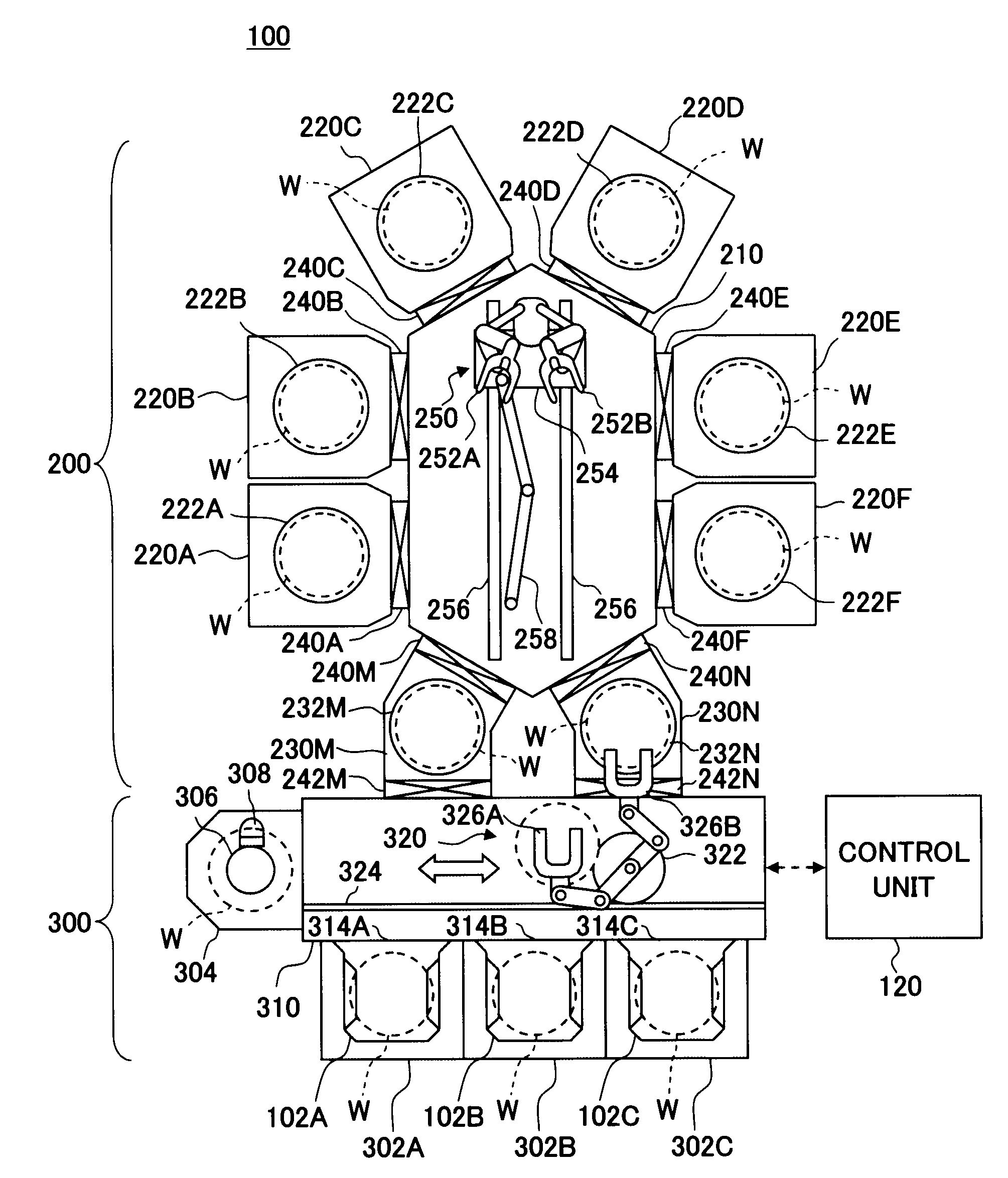
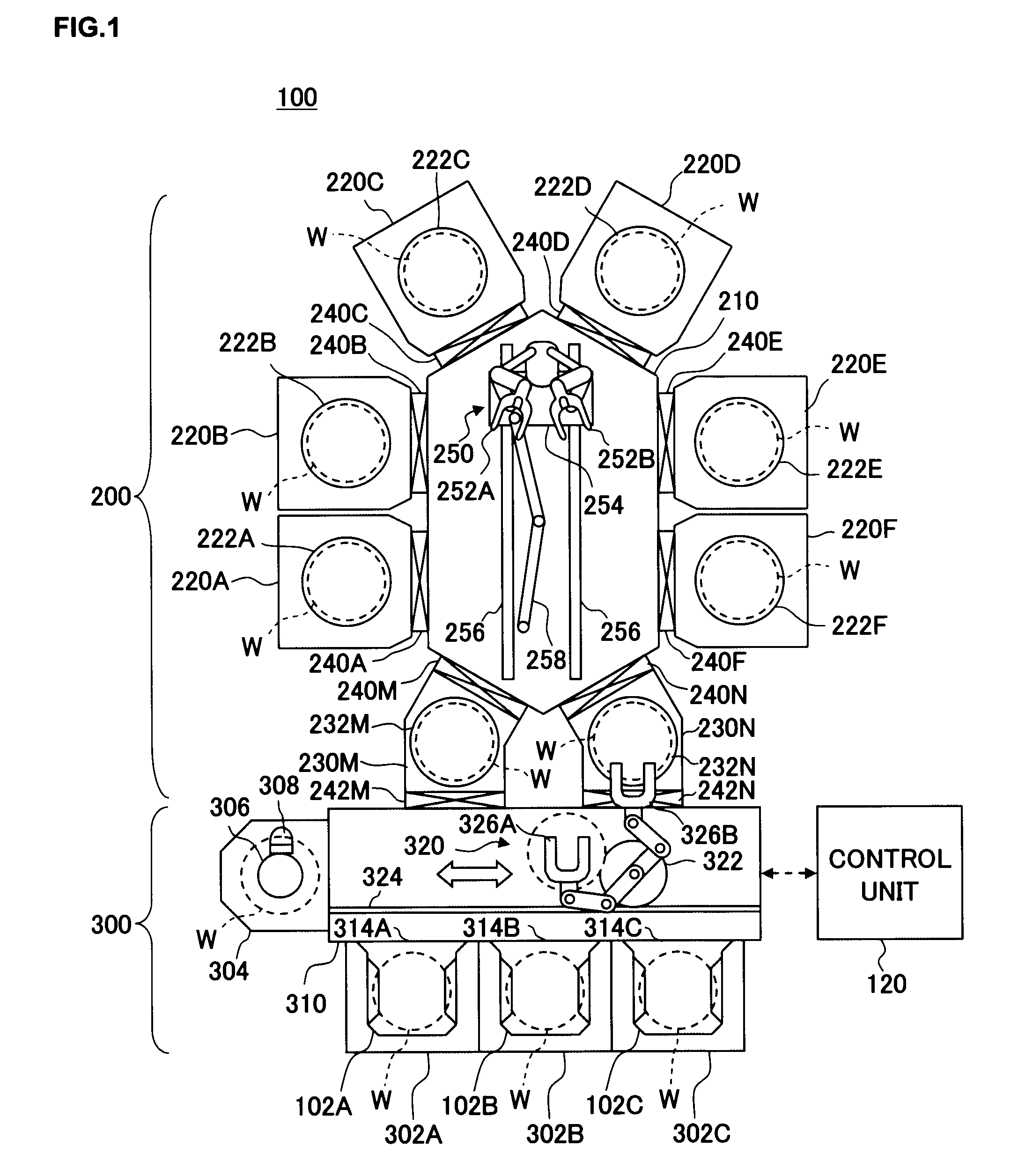
[0042]The substrate processing apparatus achieved in the embodiment of the present invention is explained first in reference to the drawings. FIG. 1 schematically illustrates the structure adopted in the substrate processing apparatus achieved in the embodiment of the present invention. The substrate processing apparatus 100 comprises a processing unit 200 equipped with a plurality of processing chambers where various types of processing such as etching and surface treatment are executed on substrates such as semiconductor wafers W in a low ...


PUM

PropertyMeasurementUnit
Temperatureaaaaaaaaaa
Pressureaaaaaaaaaa

Abstract

The present invention provides a method, an apparatus and the like that may be adopted when executing a specific type of processing on a substrate that includes a recessed portion formed by etching a low dielectric constant insulating film with a low dielectric constant having been formed upon a metal layer. More specifically, a hydrogen radical processing phase in which the surface of the metal layer exposed at the bottom of the recessed portion is cleaned and the low dielectric constant insulating film is dehydrated by supplying hydrogen radicals while heating the substrate to a predetermined temperature and a hydrophobicity processing phase in which the low dielectric constant insulating film exposed at a side surface of the recessed portion is rendered hydrophobic by supplying a specific type of processing gas to the substrate are executed in succession without exposing the substrate to air.

Description

CROSS-REFERENCE TO RELATED APPLICATIONS[0001]This document claims priority to Japanese Patent Application Number 2007-168132, filed on Jun. 26, 2007 and U.S. Provisional Application No. 60 / 971,943, filed on Sep. 13, 2007, the entire content of which are hereby incorporated by reference.FIELD OF THE INVENTION[0002]The present invention relates to a substrate processing method, a substrate processing apparatus and a recording medium.BACKGROUND OF THE INVENTION[0003]As an increasingly higher extent of integration is achieved in semiconductor integrated circuits in recent years, semiconductor devices need to adopt a multilayer wiring structure allowing wiring is to be stacked over many layers. A semiconductor device adopting a multilayer wiring structure needs to include trench wiring that connects various elements laid out along the horizontal direction and via hole wiring for connecting various elements layered along the vertical direction. A low-resistance metal with outstanding anti...

Claims


Application Information

Patent Timeline
IPC IPC(8): H01B13/00
CPCH01L21/02063H01L21/3105H01L21/76826H01L21/76814H01L21/31138
Inventor KUBOTA, KAZUHIROTAHARA, SHIGERUASAKO, RYUICHI
Owner TOKYO ELECTRON LTD
Learn More