
1T MEMS scalable memory cell

a memory cell and scalable technology, applied in the field of integrated circuits, can solve the problems of tunnel oxide, negative impact on memory retention time, gate leakage current generation, etc., and achieve the effect of reducing the leakage through the gate and reducing the memory density

Inactive Publication Date: 2008-11-13
STMICROELECTRONICS SRL
View PDF3 Cites 58 Cited by
  • Summary
  • Abstract
  • Description
  • Claims
  • Application Information

AI Technical Summary

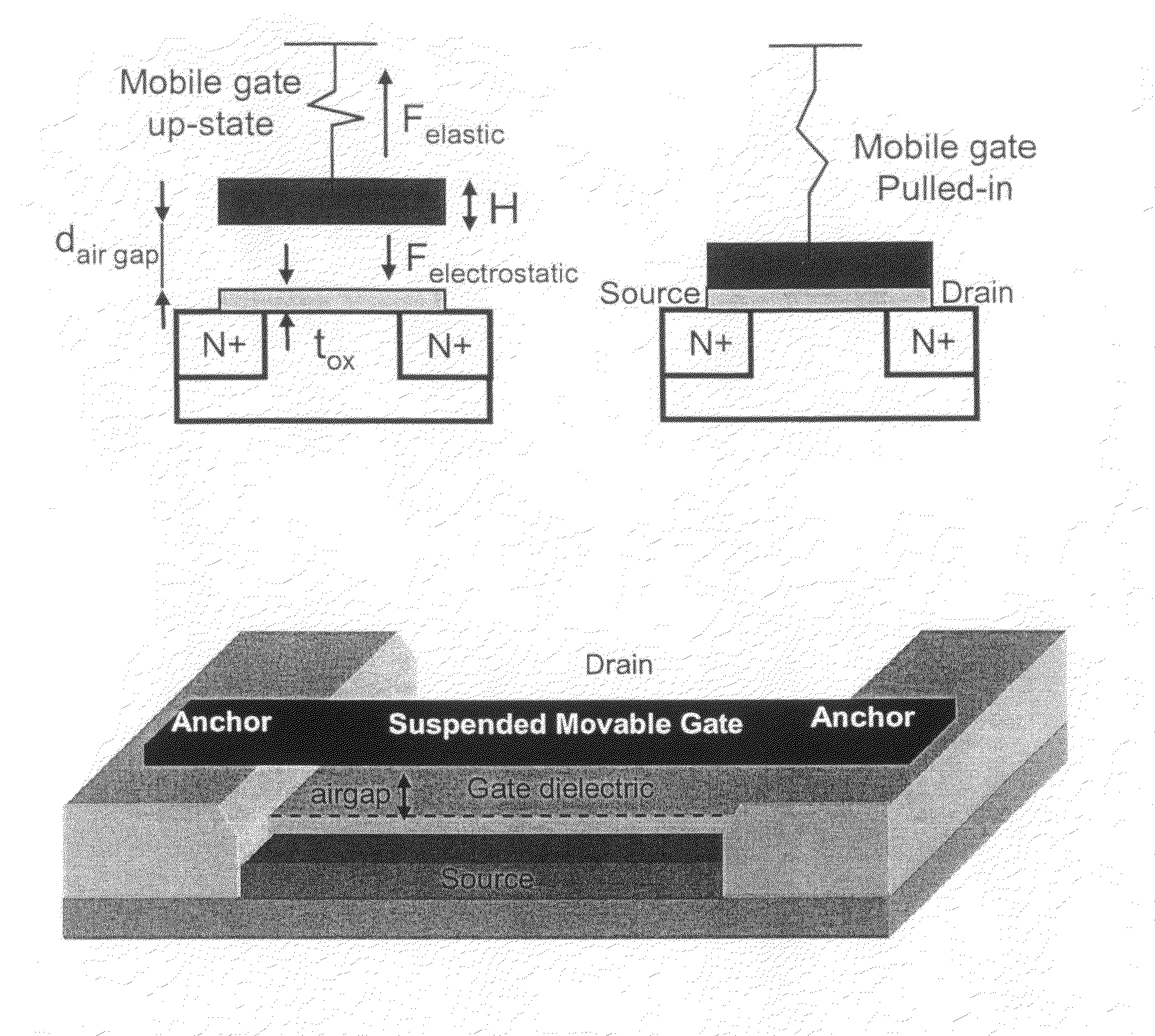
Benefits of technology

[0006]To reduce the leakage through the gate and avoid the need of very thin tunnel oxide, two inventions were disclosed describing the use of an air-gap to inject charges from a suspended conductive gate to an electrically conductive floating gate by the mechanical contact of the two surfaces (U.S. Pat. No. 6,509,605 and U.S. Pat. No. 6,054,745). The two patents describe an architecture where the actuation of the beam with an electrode and the floating gate are two different components used to actuate the gate and store charges under the beam. The separation of the actuation and storage induces a reduction of the memory density.

Problems solved by technology

Various materials and architectures of such memories have been investigated in the past but some issues still remain:Leakage current and retention time—As the gate contact is in contact with the storage region, part of the stored charges can migrate through the gate (and tunnel oxide) and generate a gate leakage current.
This can negatively impact the memory retention time.High voltages needed for electron tunneling—Large electric field is needed for electron tunneling to operate the memory, this requirement could be mirrored in a relatively high voltages compared to the small ones available in nanoscale CMOS.

Method used


Image

  • 1T MEMS scalable memory cell
  • 1T MEMS scalable memory cell
  • 1T MEMS scalable memory cell

Examples


Embodiment Construction

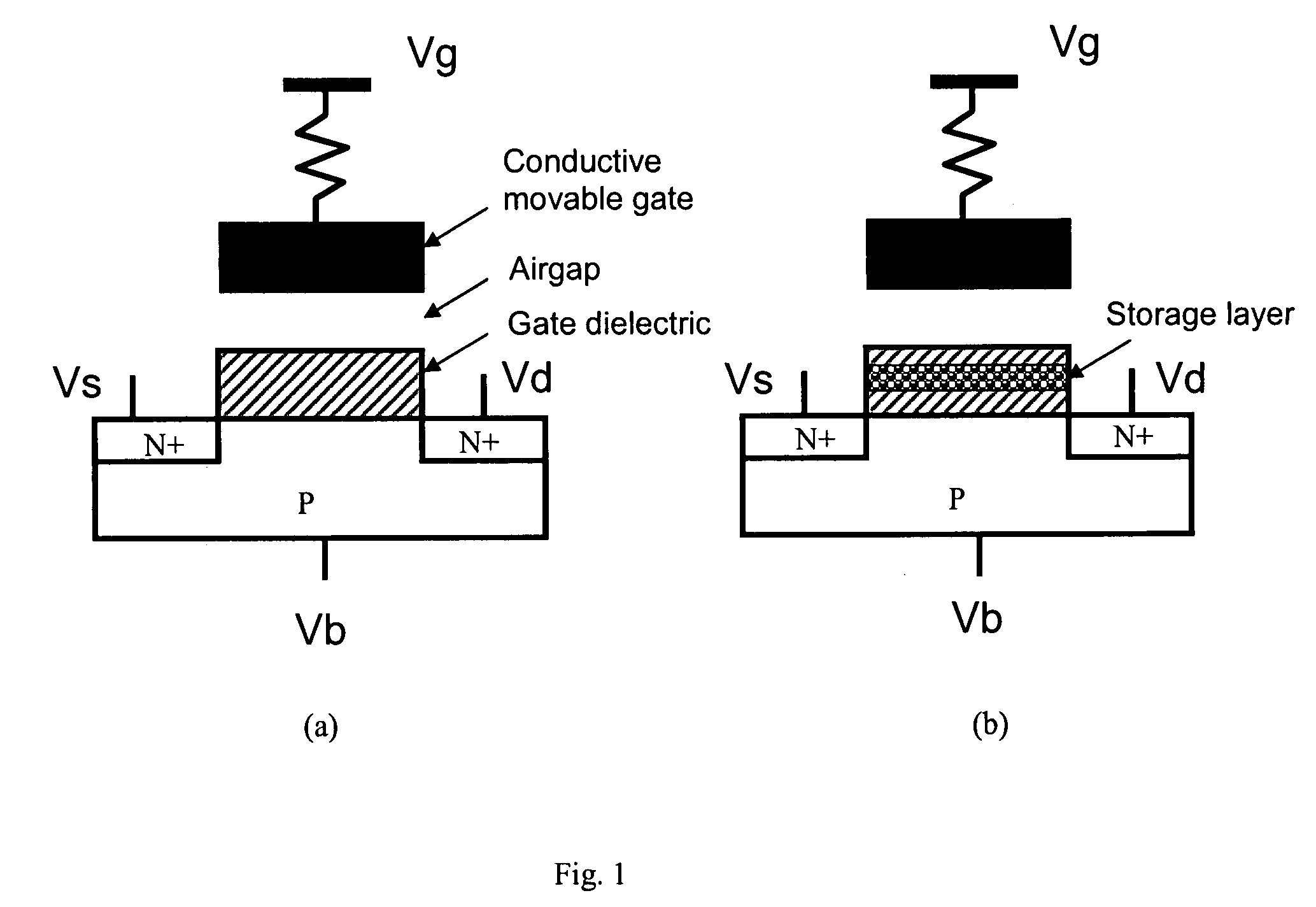
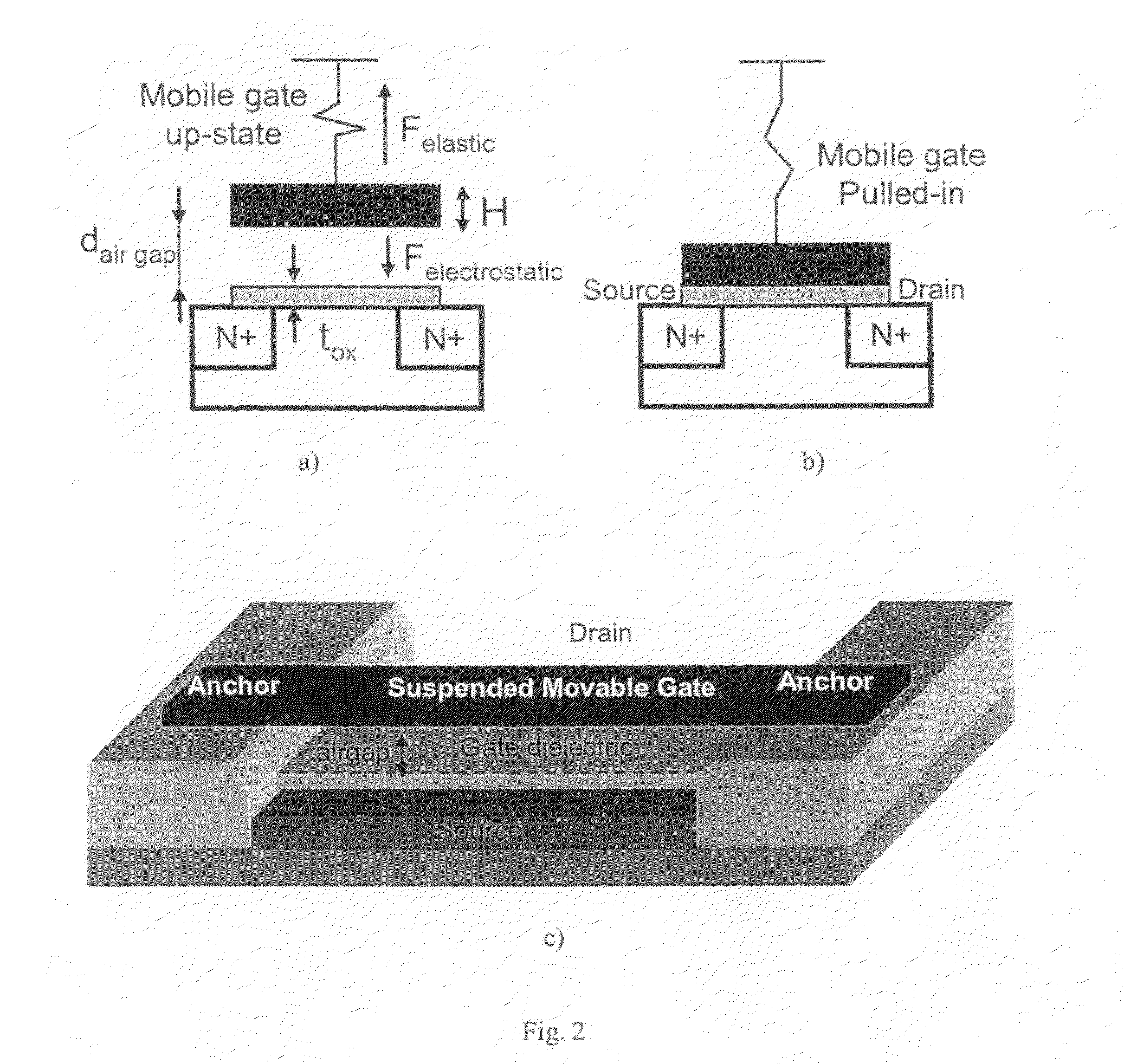
[0011]This invention proposes a new one transistor (1T) memory cell that overcomes the problem of leakage and meets high density requirements by exploiting a hybrid MEMS-MOS technology. We propose a different principle and approach for a 1T MEMS memory cell, essentially using a suspended-gate MOS transistor.

[0012]This invention proposes to use a gate dielectric placed under the mobile gate electrode of MOS transistor, without the need of the conductive floating gate mentioned by previous authors. The invention exploits the electromechanical hysteretic behavior of the mobile gate when down contacting (event called pull-in) and up separating (event called pull-out) from the gate dielectric, based on the (non)equilibrium between electrical and elastic forces. The difference between pull-in and pull-out gate voltages defines a significant memory window that can be used in volatile memory applications like SRAM and DRAM. When the gate voltage of mobile gate MOS transistor is increased, a...


PUM


Abstract

This invention relates to the use of a gate dielectric placed under the mobile gate electrode of MOS transistor, without the need of a conductive floating gate. The invention exploits the electromechanical hysteretic behavior of the mobile gate when down contacting (pull-in) and up separating (pull-out) from the gate dielectric, based on the (non)equilibrium between electrical and elastic forces.

Description

CROSS REFERENCE TO RELATED APPLICATION[0001]This application is based on, and claims domestic priority benefits under 35 U.S.C. §119(e) from, Provisional Application No. 60 / 861,731, filed Nov. 30, 2006, the entire content of which is hereby incorporated by reference.BACKGROUND OF THE INVENTION[0002]The invention concerns the integrated circuit domain and, particularly, volatile and non-volatile memories based on Micro-Electro-Mechanical devices.BRIEF SUMMARY OF THE INVENTION[0003]Floating gate memory device, like FLASH memory for example, where the memory cell is composed of the following stack: tunnel oxide, storage material and conductive controlling gate over transistor channel was adopted by industry. Charges are stored in a storage material by tunneling through a tunnel oxide when transistor is conducting. Various materials and architectures of such memories have been investigated in the past but some issues still remain:[0004]Leakage current and retention time—As the gate cont...

Claims


Application Information

Patent Timeline
Patent Type & Authority Applications(United States)
IPC IPC(8): H01L29/792H01L27/12
CPCB82Y10/00G11C13/025G11C23/00G11C2213/16H01L21/28273H01L29/40114
Inventor IONESCU, MIHAI ADRIANABELE, NICOLAS
Owner STMICROELECTRONICS SRL
Learn More