
Multispectral plasmonic crystal sensors

a plasmonic crystal and sensor technology, applied in the field of multispectral plasmonic crystal sensor, can solve the problems of difficult integration of kretschmann spr optical configuration into complex form factor devices useful for high-end applications, subject to several practical limitations, etc., and achieve the effect of improving local plasmonic field distribution

Inactive Publication Date: 2008-09-04
THE BOARD OF TRUSTEES OF THE UNIV OF ILLINOIS
View PDF11 Cites 163 Cited by
  • Summary
  • Abstract
  • Description
  • Claims
  • Application Information

AI Technical Summary

Benefits of technology

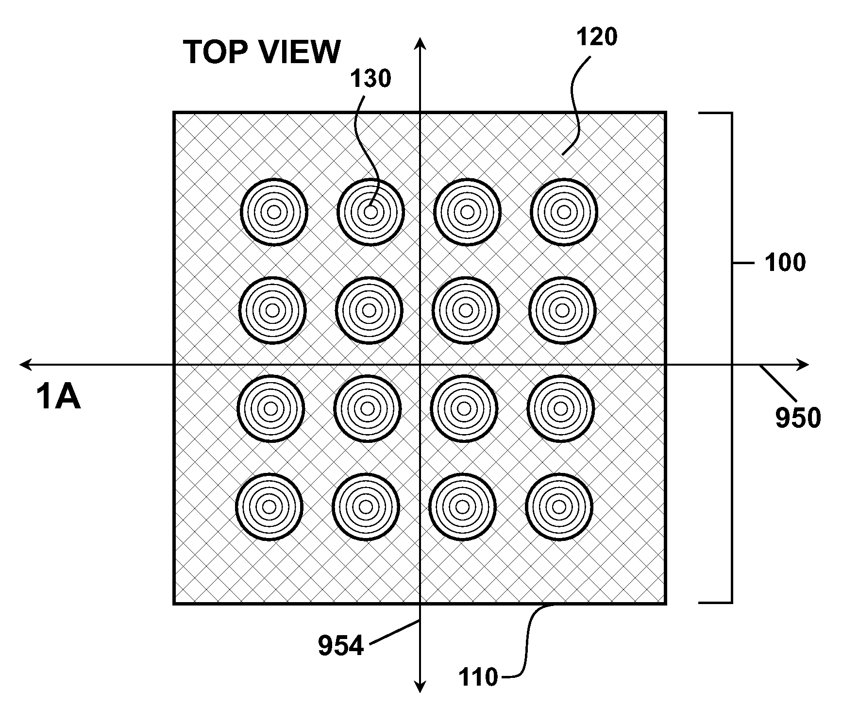
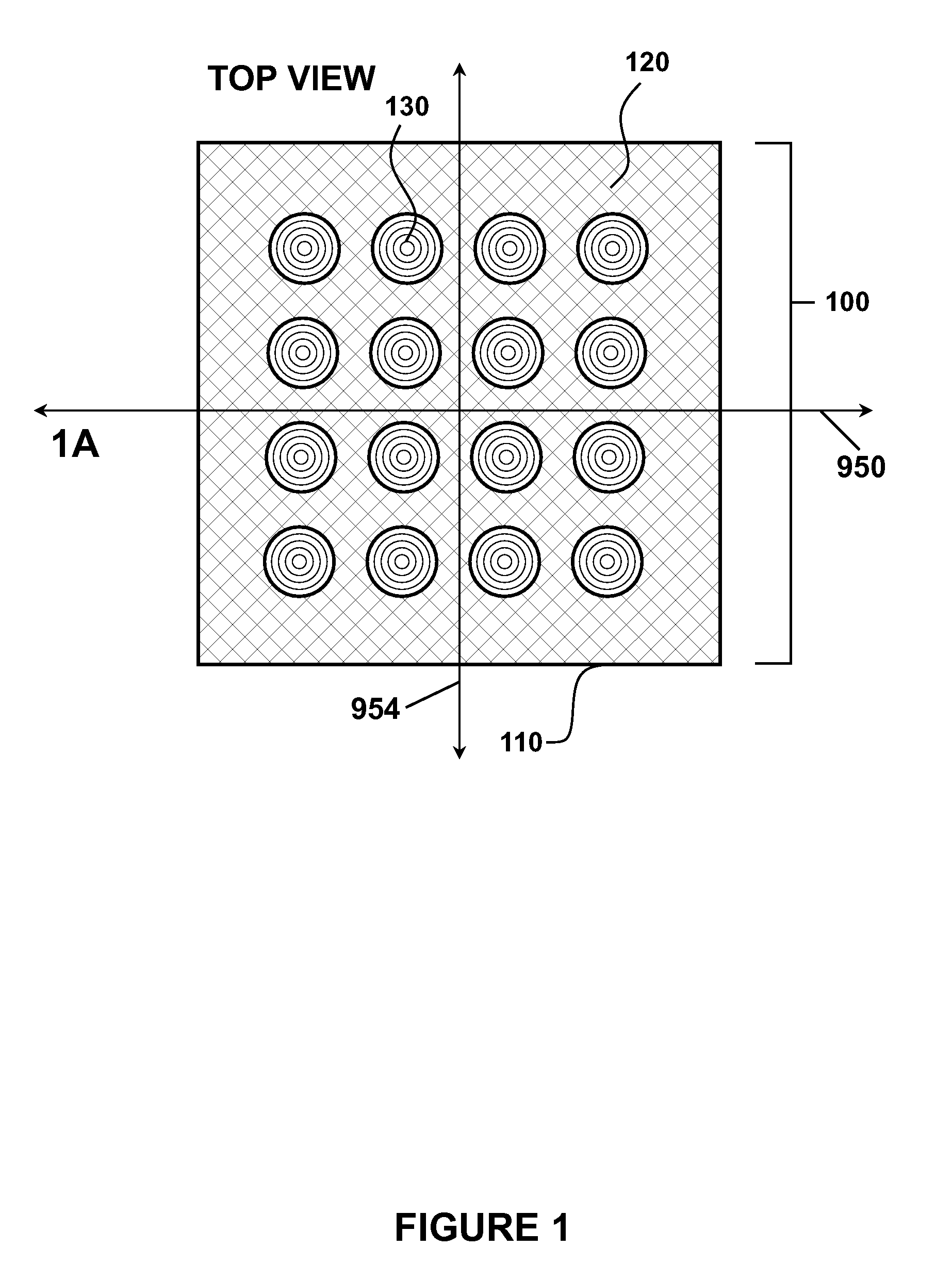
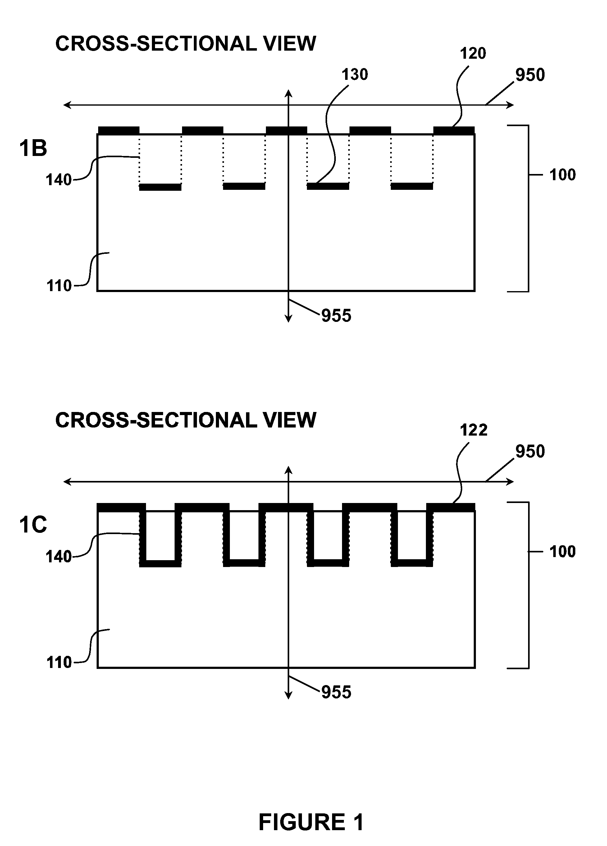
[0012]The present invention provides plasmonic crystals comprising three-dimensional and quasi comprising three-dimensional distributions of metallic or semiconducting films, including multi-layered crystal structures comprising nanostructured films and film arrays. Plasmonic crystals of the present invention include precisely registered and deterministically selected nonplanar crystal geometries and spatial distributions providing highly coupled, localized plasmonic responses in thin film elements and / or nanostructures of the crystal. Coupling of plasmonic responses provided by three-dimensional and quasi-three dimensional plasmonic crystal geometries and structures of the present invention generates enhanced local plasmonic field distributions useful for detecting small changes in the composition of an external dielectric environment proximate to a sensing surface of the plasmonic crystal. Plasmonic crystal structures of the present invention are also useful for providing highly localized excitation and / or imaging of fluorophores proximate to the crystal surface.
[0013]Plasmonic crystals of the present invention enable a robust optical sensing platform for high performance chemical and biological sensing. Sensors, sensing methods and sensing systems of the present invention are capable of multispectral spectroscopic SPR sensing and / or spatially resolved SPR imaging for detecting and characterizing the optical properties, chemical compositions and / or physical properties of variety of materials. Sensors of the present invention are compatible with compact form factors and are capable of direct, low cost integration into a range of delivery and high throughput screening systems, including microfluidic, nanofluidic and microarray systems and formats. Sensors and sensing methods of the present invention provide exceptional sensitivities (e.g., Figure of Merit ranging from about 100 nm / RI to about 700 nm / RI), good spatial resolution imaging and are capable of label-free quantitative detection of a wide variety of analytes, including biological molecules and therapeutic drug candidates. In some embodiments wherein full multispectral intensity is accessed during measurement, sensitivities on the order of 22,000 nm·% T RI−1 are achievable for a photonic crystal sensor of the present invention having a photonic crystal with a multilayer film geometry and sensitivities on the order of 44,000 nm·% T RI−1 are achievable for a photonic crystal sensor of the present invention having a photonic crystal with a continuous film geometry.
[0014]The present invention also provides methods for fabricating plasmonic crystals via a combination of soft lithographic patterning and thin film deposition techniques. Processing methods of the present invention provide a versatile, low cost and commercially attractive imprinting-based or replica molding-based fabrication platform for making two-, three- and quasi three-dimensional plasmonic crystals having preselected thin film and / or nanostructured geometries, including three-dimensional multilayered crystal geometries. The present plasmonic crystal fabrication methods enable non-planar integration of precisely registered thin film elements having accurately selected physical dimensions and spatial orientations. Processing methods of the present invention access two-, three- and quasi three dimensional plasmonic crystal geometries comprising thin film element arrays and feature arrays having one or more physical dimensions (e.g., length, width, thickness, diameter, radius etc.) ranging from 10s of nanometers to 1000s of microns.

Problems solved by technology

The Kretschmann SPR optical configuration, while highly sensitive (a Figure of Merit, FOM, of greater than about 1000 nm / R1 is typical), is subject to several practical limitations.
First, it is difficult to integrate theses optical configurations into complex form factor devices useful for high throughput fluidic screening applications, including microfluidic (μFl) and nanofluidic (nFl) systems for bioanalytical measurement.
Kretschmann geometry based sensors assemblies using angle of incidence modulation require complex and spatially restrictive rotation assembles that are prohibitive for some applications and require frequent realignment and optimization.
Second, the mechanical integrity of these systems may not be robust enough for important large-area, array-based screening applications.
These architectures require, however, external optical systems through which the array / nanoparticles can be spectroscopically interrogated, and therefore are less attractive for large-area, array-based screening applications.
Further, significant deviations in nanoparticle positions and sizes provide practical limitations on the use of nanoparticle arrays for SPR sensing.
While surface plasmon responses accessed using metal thin films is well established, application of these structures for SPR sensing has not yet been fully explored.

Method used


Image

  • Multispectral plasmonic crystal sensors
  • Multispectral plasmonic crystal sensors
  • Multispectral plasmonic crystal sensors

Examples


example 1

High Performance Plasmonic Crystal Sensor Formed by Soft Nanoimprint Lithography

Abstract

[0117]This Example describes a new type of plasmonic sensor fabricated by imprint lithography using a soft, elastomeric mold. Angle-dependent, zero-order transmission experiments demonstrate the sensing potential of this device, which uses a two dimensional plasmonic crystal. Full angle-dependent mapping shows that the sensitivity to surface chemical binding events reaches maxima near regions of the plasmonic Brillouin zone where the dispersion curves of multiple surface plasmon polariton modes converge. This behavior, together with the simple, low cost procedures for building the structures, demonstrates an important role for these devices in high performance chemical and biological sensing.

Introduction

[0118]The field of biosensing exploits many technologies that are optically based. While heavily dominated by spectroscopic protocols that employ fluorescence, label-less methods that exploit the ...

experiment & results

[0122]We performed zero-order transmission experiments in order to obtain the PBZ map of these structures. The scheme of the setup is presented in FIG. 5. The sample was fixed on a 2-axis rotation stage mounted inside of a UV-Vis-NIR spectrophotometer (Cary 5G). One axis turned the device to the required polar angle of incidence θ. The other rotated the sample around the Z axis (FIG. 5). This stage defines the direction for excitation and propagation of the plasmonic modes on the metal surface. The transmission spectra have a nominal spectral resolution of 1 nm, and are collected in a dual beam configuration to account for any intensity fluctuations in the light source.

[0123]PBZ maps were acquired by fixing the desired polar angle of incidence (θ) and recording a transmission spectrum over a predefined wavelength range. The angle θ was varied between 0° and 75° with incremented steps of 0.5°. Two main directions inside PBZ were mapped. One corresponded to the Γ-X direction (sample r...

example 2

Quantitative Multispectral Biosensing and Imaging Using 3D Plasmonic Crystals

Abstract

[0133]We have developed a class of three dimensional plasmonic crystal that consists of multi-layered, regular arrays of sub-wavelength metal nanostructures. When coupled with quantitative electrodynamics modeling of their optical response, these crystals enable full multi-wavelength spectroscopic detection of molecular binding events with sensitivities that correspond to small fractions of a monolayer. The high degree of spatial uniformity in the crystals, which are formed by a soft nanoimprint technique, provides the ability to image these binding events with micron spatial resolution. These features, together with compact form factors, low cost fabrication procedures, simple readout apparatus, and ability for direct integration into microfluidic networks and arrays, suggest promise for these devices in label free bioanalytical detection systems.

Background and Results

[0134]Macromolecular biologica...


PUM


Abstract

The present invention provides plasmonic crystals comprising three-dimensional and quasi comprising three-dimensional distributions of metallic or semiconducting films, including multi-layered crystal structures comprising nanostructured films and film arrays. Plasmonic crystals of the present invention include precisely registered and deterministically selected nonplanar crystal geometries and spatial distributions providing highly coupled, localized plasmonic responses in thin film elements and / or nanostructures of the crystal. Coupling of plasmonic responses provided by three-dimensional and quasi-three dimensional plasmonic crystal geometries and structures of the present invention generates enhanced local plasmonic field distributions useful for detecting small changes in the composition of an external dielectric environment proximate to a sensing surface of the plasmonic crystal. Plasmonic crystal structures of the present invention are also useful for providing highly localized excitation and / or imaging of fluorophores proximate to the crystal surface.

Description

CROSS-REFERENCE TO RELATED APPLICATIONS[0001]This application claims priority under 35 U.S.C. 119(e) to U.S. provisional Patent Application 60 / 820,254 filed Jul. 25, 2006, which is hereby incorporated by reference in its entirety.STATEMENT REGARDING FEDERALLY SPONSORED RESEARCH OR DEVELOPMENT[0002]This invention was made with government support awarded by the following agencies: DOE grant DEFG02-91-ER45439. The United States government has certain rights in the invention.BACKGROUND OF INVENTION[0003]Over the last decade, surface plasmon resonance (SPR) microscopy has emerged as a broadly applicable analytical tool for detecting and characterizing chemical and physical changes occurring in a highly localized probed region. Compatible with a wide range of condensed phase and gas phase environments, SPR is a virtually universally applicable sensing platform. In addition, SPR methods provide high detection sensitivities and excellent temporal resolution, and are compatible with a number...

Claims


Application Information

Patent Timeline
IPC IPC(8): G01N21/55G02F1/00
CPCG01N21/554
Inventor NUZZO, RALPH G.ROGERS, JOHN A.MACK, NATHAN H.STEWART, MATTHEWMALYARCHUK, VIKTORYAO, JIMIN
Owner THE BOARD OF TRUSTEES OF THE UNIV OF ILLINOIS
Learn More