
Exposure mask and method of forming pattern

a technology of mask and pattern, applied in the field of lithography process improvement, can solve the problems of reducing resolution, reducing the practical aspect, fogged pattern (a projection image) to be projected in the resist film, etc., and achieves the effects of reducing stress on the light shielding element, improving the resolution of the resist pattern, and high resolution

Inactive Publication Date: 2008-07-24
ELPIDA MEMORY INC
View PDF5 Cites 8 Cited by
  • Summary
  • Abstract
  • Description
  • Claims
  • Application Information

AI Technical Summary

Benefits of technology

[0022]By making the thickness of the light shielding element pattern of the reticle mask lager, an effect to improve resolution of the resist pattern is achieved. Further, since high resolution is kept, an effect to make a depth of focus (DOF) lager is achieved. Moreover, when the light shielding element has a laminated structure, stress on the light shielding element can be reduced, whereby an effect to heighten a processing yield of the mask is achieved. In addition, an error caused by distortion due to stress at the pattern formation can be made smaller, whereby an effect to heighten pattern accuracy is achieved. Furthermore, by adopting a damascene structure for formation of the light shielding element, an effect that a light shielding element pattern having a high aspect ratio can be formed is achieved. A method of processing a film to be processed after transcribing a thin resist pattern into another layer has an effect that a relatively thick member can be processed with a high accuracy thin film resist pattern. Thus, a reticle mask suitable for fine processing and a pattern forming method of a semiconductor device can be obtained.

Problems solved by technology

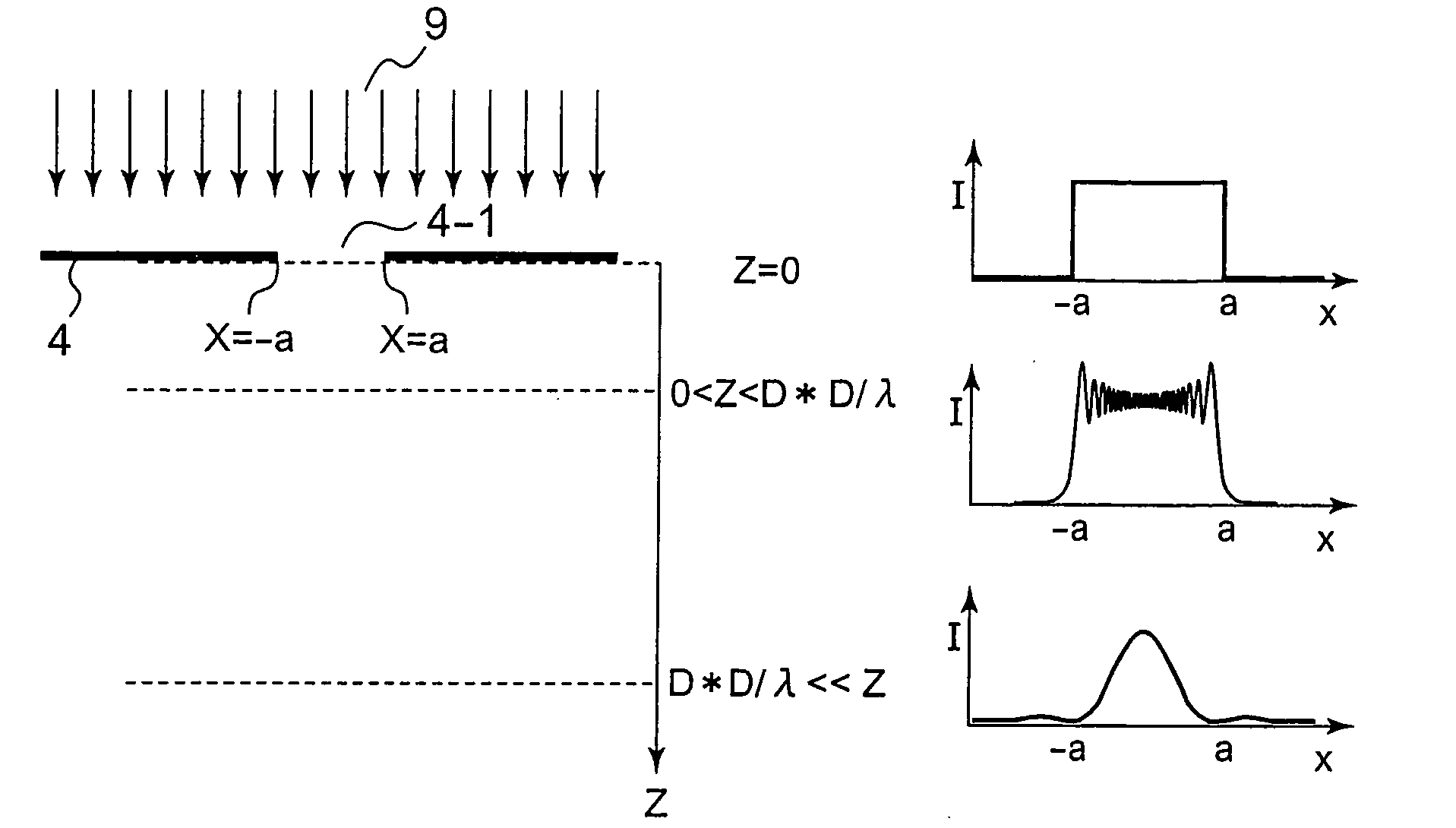
As described above, in the related art, in the case where the thickness of the light shielding element is smaller and the thickness of the resist film is larger, there is a problem that a pattern (a projection image) to be projected in the resist film is fogged and widely deformed due to diffraction of the exposing light (problem 1).
As a result, there is a problem that the depth of focus is smaller in view of the practical aspect (problem 2).
Further, there is a problem that resolution is lowered because the thickness of the resist film is made larger in associated with processing of the film to be processed (problem 3).

Method used


Image

  • Exposure mask and method of forming pattern
  • Exposure mask and method of forming pattern
  • Exposure mask and method of forming pattern

Examples


first embodiment

[0057]A first embodiment of the present invention will be described with reference to FIGS. 3 to 5. The first embodiment is an example of a pattern forming method. FIG. 3 schematically shows an exposure form in the related art. FIG. 4 schematically shows an exposure form in the present invention.

[0058]Although an illustration is omitted, a reticle mask and a semiconductor substrate are first prepared to be mounted on a stepper. In the reticle mask, a light shielding element pattern 4 (4′) is patterned on a reticle substrate 2. In the semiconductor substrate, a thin film to become a film to be processed is formed, and a resist film 8 (8′) having a predetermined thickness is formed on the film to be processed.

[0059]In FIG. 3 in which the related art is shown, the thickness of the light shielding element pattern 4′ is smaller, while the thickness of the resist film 8′ is larger.

[0060]On the other hand, in FIG. 4 in which the first embodiment of the present invention is shown, the thick...

second embodiment

[0071]A second embodiment of the present invention will be described with reference to FIGS. 6A to 6D. In the second embodiment, a thickness of a light shielding element pattern of a reticle mask is made larger, while the aspect ratio becomes larger. The second embodiment is an example in which the present invention is applied to the reticle mask used in the present invention. FIG. 6A is a plan view of a scaling reticle mask. FIG. 6B is a sectional view taken along the line A-A′ of FIG. 6A. FIG. 6C shows a plan view of the reticle mask (normal reticle mask) used in the related art. FIG. 6D shows a sectional view taken along the line B-B′ of FIG. 6C.

[0072]In an exposure reticle mask, a light shielding element pattern 4 is formed on a reticle substrate 2. In the second embodiment, “m” denotes a reciprocal number of a reduced projection ratio, “tr” denotes a thickness of a resist film, “t0” denotes a thickness of a light shielding element pattern, “D” denotes a minimum opening dimensio...

third embodiment

[0078]A third embodiment of the present invention will be described with reference to FIGS. 7A to 7F through FIGS. 12A to 12D. In the third embodiment, the thickness of the light shielding element pattern of the reticle mask becomes larger and the aspect ratio becomes larger. Therefore, the third embodiment is an example in which a configuration of the light shielding element pattern in the reticle mask is improved.

[0079]The light shielding element of the reticle mask can be constructed from a single member as explained with reference to FIGS. 6A to 6D. However, the light shielding element is not limited to this, and it can be constructed from a plurality of light shielding layers.

[0080]FIGS. 7A to 7F respectively show sections of various reticle masks constructed from a plurality of light shielding layer. The total thickness of the plurality of light shielding layers is set so as to become the thickness t0 that meets the conditional equations described above. The light shielding el...


PUM


Abstract

A method of forming a pattern according to the present invention comprising preparing a reduced projection exposure apparatus having a reduced projection ratio 1 / m and a wavelength λ (nm) of exposing light and patterning a light shielding element pattern of a reticle mask on a resist film having a thickness tr (nm). The light shielding element pattern has a pattern opening portion having a minimum opening dimension D (nm). A thickness t0 of the light shielding element pattern is set so as to meet a relational equation of m*tr≦t0+5*D*D / λ. Preferably, the thickness t0 of the light shielding element pattern is set so as to meet a relational equation of m*tr≦t0+D*D / λ.

Description

[0001]This application is based upon and claims the benefit of priority from Japanese patent application No. 2007-11461, filed on Jan. 22, 2007, the disclosure of which is incorporated herein in its entirety by reference.FIELD OF THE INVENTION[0002]The present invention relates to improvement of a lithography process when manufacturing a semiconductor device and, in particular, to an exposure mask and a method of forming a pattern of the semiconductor device which are used for a fine dimension of a submicron region.BACKGROUND OF THE INVENTION[0003]With the recent development of a manufacturing technology of a semiconductor device, a semiconductor device in which elements are integrated with high density has come into practical use. For example, in a Dynamic Random Access Memory, a memory having a storage capacity of 1 Gbit has come into practical use. With the high integration of the semiconductor device, an element pattern is to be miniaturized. Although a current minimum processin...

Claims


Application Information

Patent Timeline
IPC IPC(8): G03F1/00G03F7/26G03F1/30G03F1/32G03F1/68H01L21/027
CPCG03F1/144G03F1/68G03F1/32G03F1/26
Inventor SAITO, MASAYOSHI
Owner ELPIDA MEMORY INC
Learn More