Aromatic enediyne derivative, organic semiconductor thin film, electronic device and methods of manufacturing the same

a technology of organic semiconductors and derivatives, applied in the direction of thermoelectric devices, sustainable manufacturing/processing, final product manufacturing, etc., can solve the problems of reducing voltage, difficult to implement in the actual device fabrication line, and unsuitable for inexpensive preparation of films having a relatively large area

Active Publication Date: 2008-05-22
SAMSUNG ELECTRONICS CO LTD
View PDF1 Cites 8 Cited by
  • Summary
  • Abstract
  • Description
  • Claims
  • Application Information

AI Technical Summary

Problems solved by technology

In this regard, the low-molecular-weight organic material, e.g., pentacene, has been reported to have increased charge mobility of about 3.2 cm2/Vs˜about 5.0 cm2/Vs or more and an improved on/off current ratio, but suffers because the low-molecular-weight organic material may require an expensive apparatus for vacuum deposition upon formation of a thin film and may be difficult to use to form a fine pattern, and therefore may be unsuitable for inexpensive preparation of a film having a relatively large area.
However, such ...

Method used


Image

  • Aromatic enediyne derivative, organic semiconductor thin film, electronic device and methods of manufacturing the same
  • Aromatic enediyne derivative, organic semiconductor thin film, electronic device and methods of manufacturing the same
  • Aromatic enediyne derivative, organic semiconductor thin film, electronic device and methods of manufacturing the same

Examples


example 1

Preparation of Organic Semiconductor Thin Film

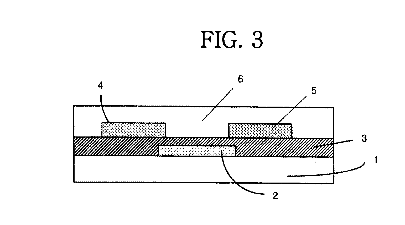
[0052]On a washed plastic substrate, aluminum / niobium (Al / Nb) alloy for a gate electrode was deposited to about 1000 Å through sputtering, and then SiO2 for a gate insulating film was deposited to about 1000 Å using CVD.

[0053]Subsequently, Au for source / drain electrodes was deposited to about 1200 Å thereon through sputtering. Before being coated with the organic semiconductor material, the substrate was washed using isopropyl alcohol for about 10 min and then dried. The sample was dipped into a about 10 mM octadecyltrichlorosilane solution in hexane for about 30 sec, washed with acetone, and then dried. Thereafter, the aromatic enediyne derivative of Preparative Example 1 was dissolved to about 0.1 wt % in a xylene solvent, applied on the substrate via dropping, and then baked at about 100° C. for about 30 min in an argon atmosphere, thereby fabricating the bottom-contact-type OTFT as seen in FIG. 3.

example 2

Fabrication of OTFT

[0054]An OTFT was fabricated in the same manner as in Example 1, with the exception that, in the annealing process, the baking was conducted at about 160° C. for about 30 min.

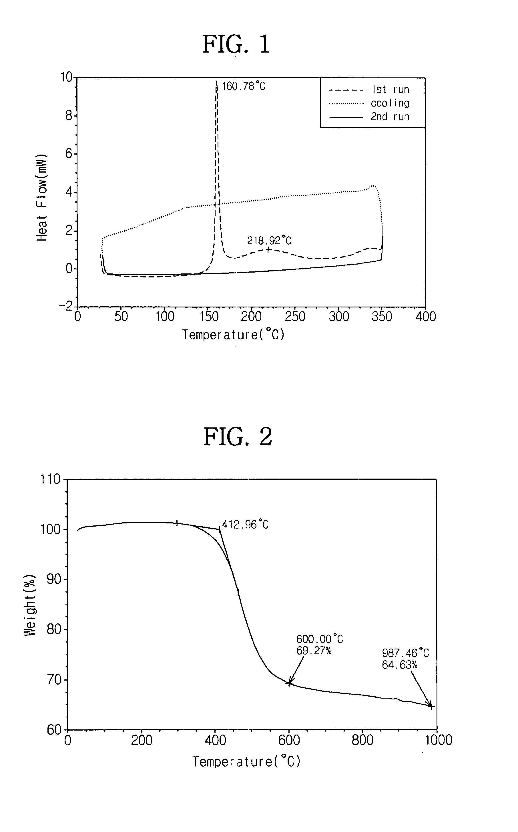
[0055]The DSC of the aromatic enediyne derivative synthesized in Preparative Example 1 was measured. The results are shown in FIG. 1.

[0056]As shown in FIG. 1, the aromatic enediyne derivative of example embodiments was found to begin to crosslink at about 150° C. and then to actively react at about 170° C. or lower. As is apparent from these results, the aromatic enediyne derivative of example embodiments may be formed into a semiconductor thin film through a low-temperature wet process.

[0057]Further, the TGA of the aromatic enediyne derivative of Preparative Example 1 was measured. The results are shown in FIG. 2.

[0058]As seen in FIG. 2, the aromatic enediyne derivative of example embodiments did not lose any weight up to about 300° C. The aromatic enediyne derivative of example embodiments ...


PUM


Abstract

Disclosed are a novel aromatic enediyne derivative, an organic semiconductor thin film using the same, and an electronic device. Example embodiments pertain to an aromatic enediyne derivative which enables the formation of a chemically and electrically stable and reliable semiconductor thin film using a solution process, e.g., spin coating and/or spin casting, at about room temperature when applied to devices, an organic semiconductor thin film using the same, and an electronic device including the organic semiconductor thin film. A thin film having a relatively large area may be formed through a solution process, therefore simplifying the manufacturing process and decreasing the manufacturing cost. Moreover, it is possible to provide an organic semiconductor that may be effectively applied to various fields including organic thin film transistors, electroluminescent devices, solar cells, and memory.

Description

PRIORITY STATEMENT[0001]This non-provisional application claims priority under U.S.C. § 119 to Korean Patent Application No. 2006-0113845, filed on Nov. 17, 2006, in the Korean Intellectual Property Office, the entire contents of which are herein incorporated by reference.BACKGROUND[0002]1. Field[0003]Example embodiments relate to an aromatic enediyne derivative, an organic semiconductor thin film, an electronic device and methods of manufacturing the same. Other example embodiments relate to an aromatic enediyne derivative, an organic semiconductor thin film, which may be prepared from the aromatic enediyne derivative through a solution process, e.g., spin coating and / or spin casting, at about room temperature, and has improved chemical and electrical stability and reliability, an electronic device comprising the organic semiconductor thin film and methods of manufacturing the same.[0004]2. Description of the Related Art[0005]In general, flat display devices, e.g., liquid crystal d...

Claims


Application Information

Patent Timeline
IPC IPC(8): H01L51/40C07D495/02H01L51/00
CPCC07D495/04C07F7/0812H01L51/0056Y02E10/549H01L51/0074H01L51/0094H01L51/0545H01L51/0058Y02P70/50H10K85/624H10K85/626H10K85/6576H10K85/40H10K10/466H10K99/00H10K10/00
Inventor JEONG, EUN JEONGMOON, HYUN SIKPARK, JEONG ILLEE, SANG YOON
Owner SAMSUNG ELECTRONICS CO LTD
Why Eureka
Try Eureka